Cartridge
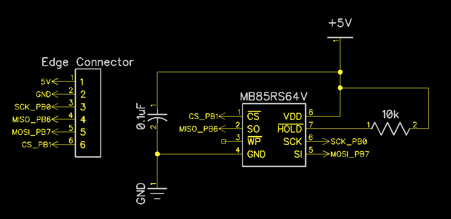
Circuit Diagram
Background
The game cartridge uses an 8KB FRAM chip for storage. The chip is communicated with over SPI rather than being connected directly to the bus. The tradeoff with using an SPI memory module is that there is a time delay for loading the game, but the design is simple. To use SPI with a 65C22, 4 pins are needed. The 65C22 has no hardware support specifically for SPI, so the protocol must be bit-banged.
| Pin | Description |
|---|---|
| PB0 | Clock - Using this pin means, INC and DEC can be used to oscillate the clock signal easily |
| PB1 | Chip Select - For FRAM |
| PB6 | MOSI - Write out bits on this pin |
| PB7 | MISO - Reading from bit 7 easy with the BIT operator. BIT sets S flag based on value of bit 7. |
PB2 - PB5 are still available for other purposes, or to be the chip select for 4 additional SPI devices.
The cartridge is designed to be reversible. It does not matter which way it is inserted into the connector.
Components
| Component | Description | Image |
|---|---|---|
| Edge Connector | 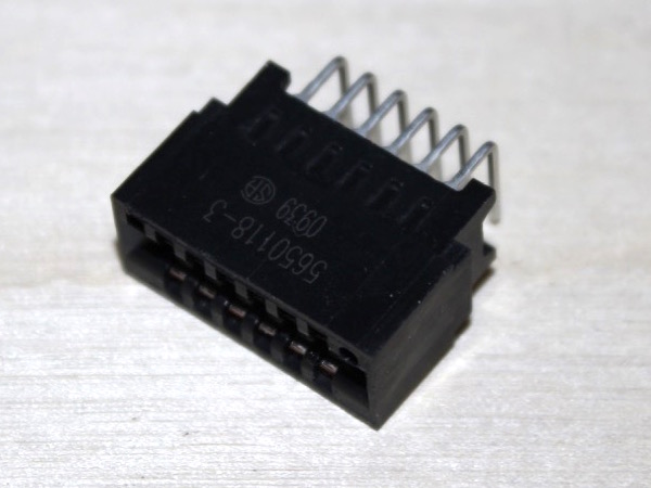 |
|
| Game Cartridge | 8KB FRAM Cartridge | 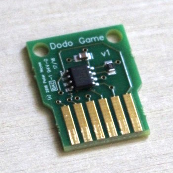 |