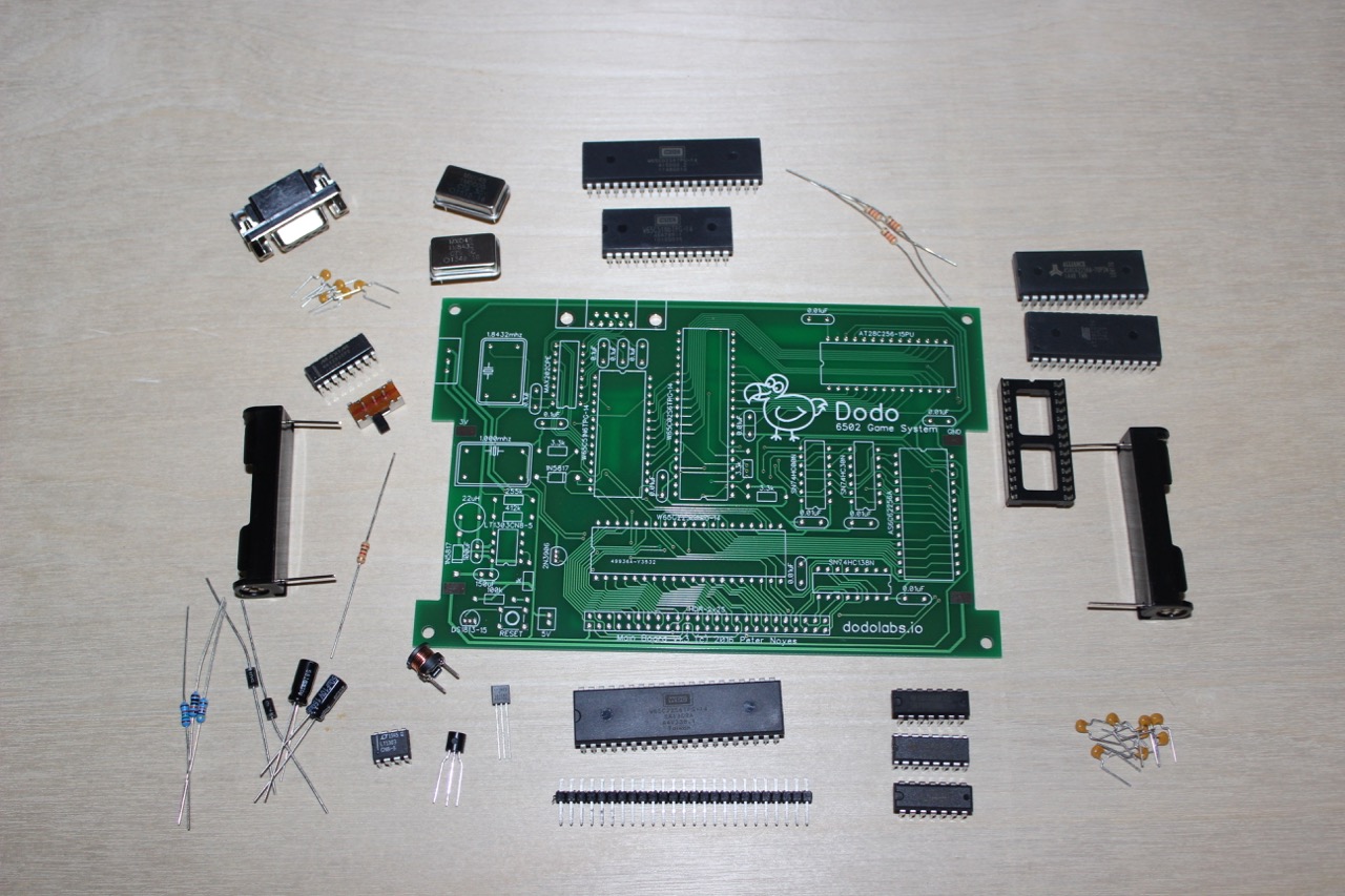
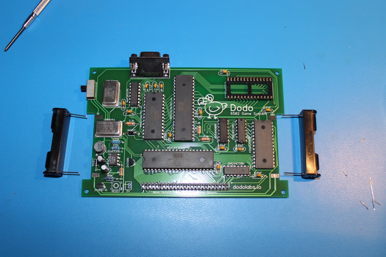
Assembly
It is recommended to be familiar with soldering before attempting this kit. Here are some general soldering tips:
- Solder flows toward heat. Use this to your advantage by heating the plated hole as best as possible and pushing the solder into the joint. Heating just the lead will cause the solder to bead instead of flowing into the hole.
- Have a small amount of solder on the tip before soldering
- Do not use a wet sponge, instead use a brass cleaning sponge, this way you will not lose any heat.
- If using lead free solder, set to 750 degrees
Step 1 - ICs
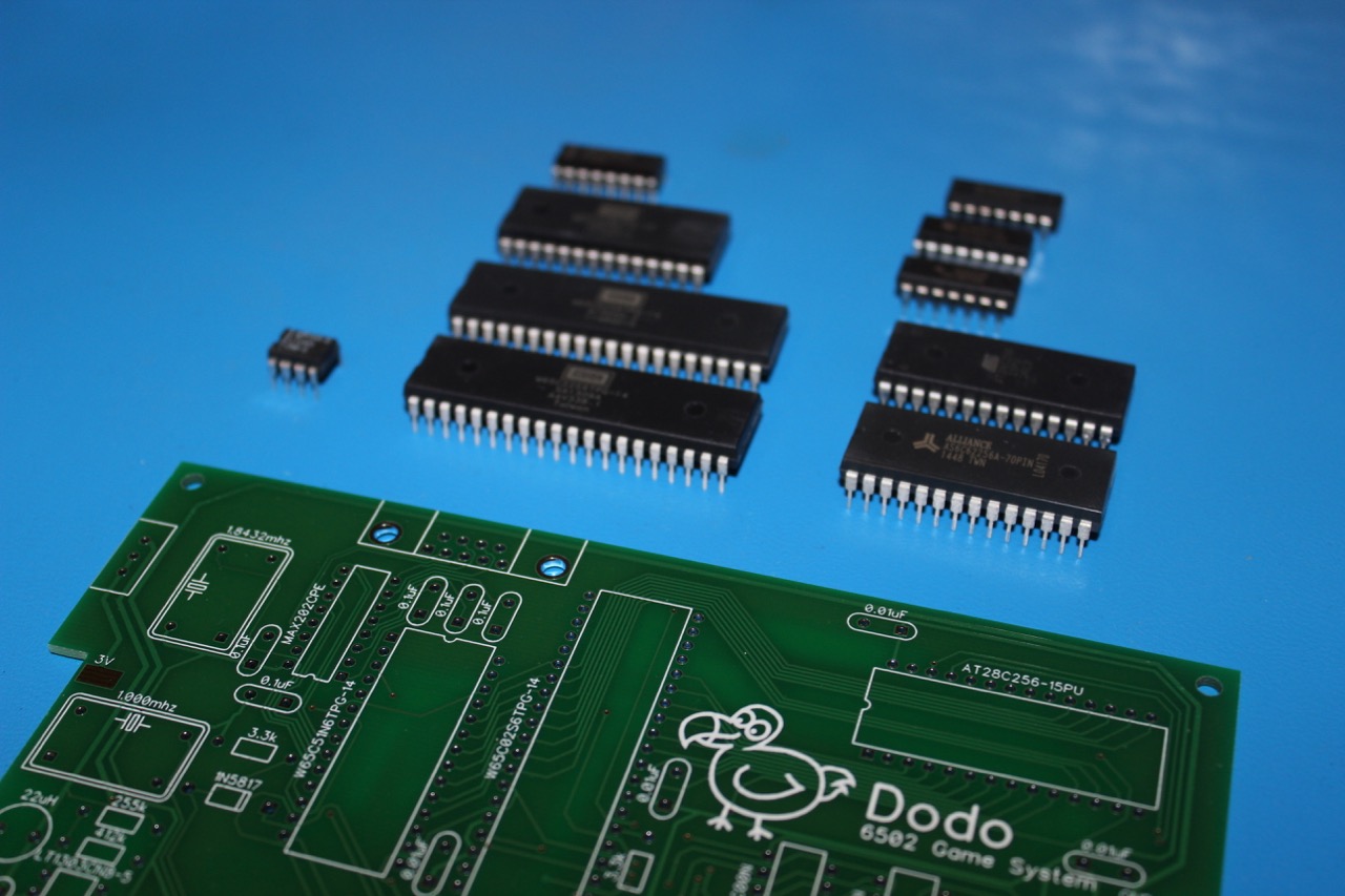
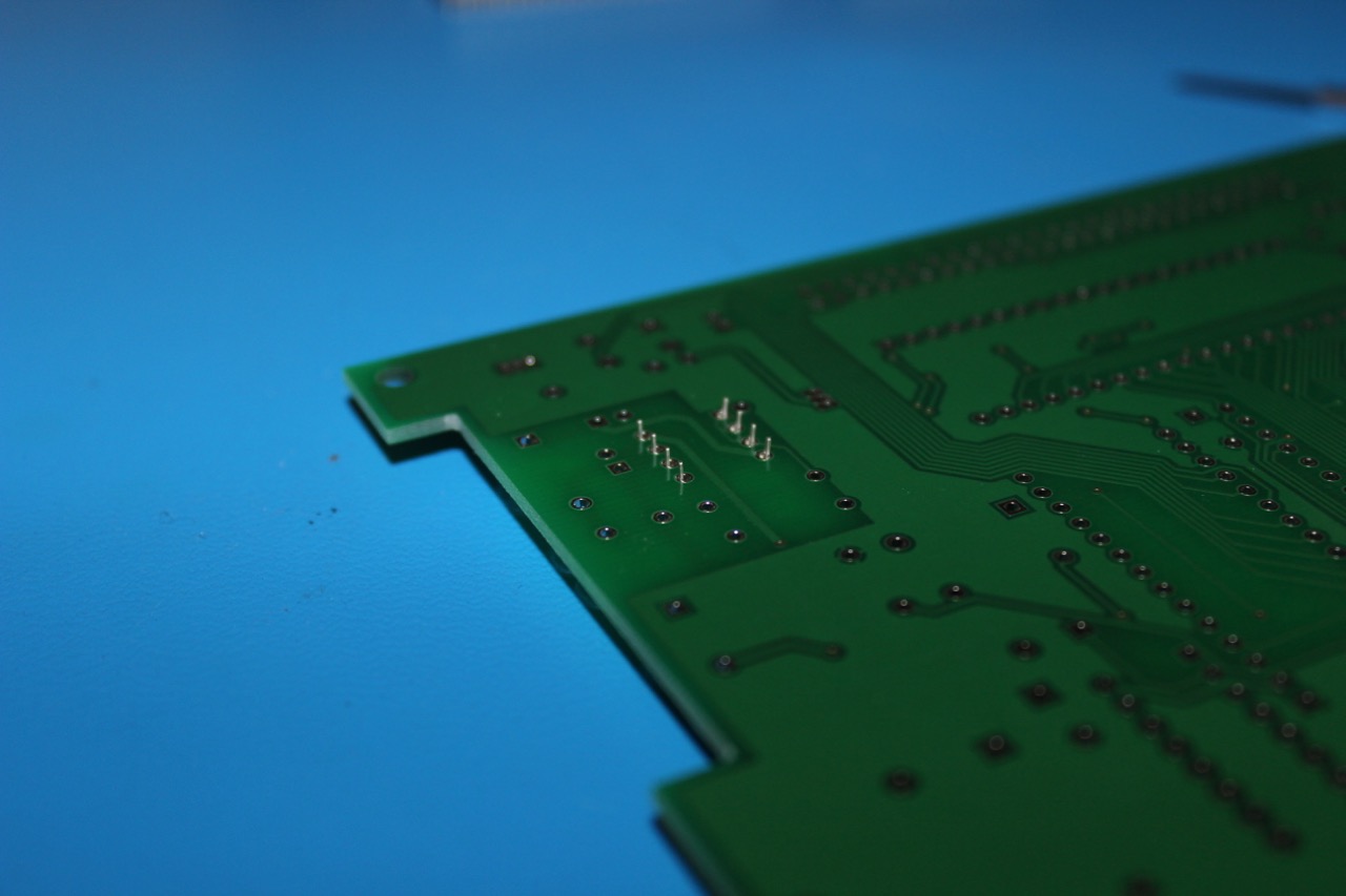
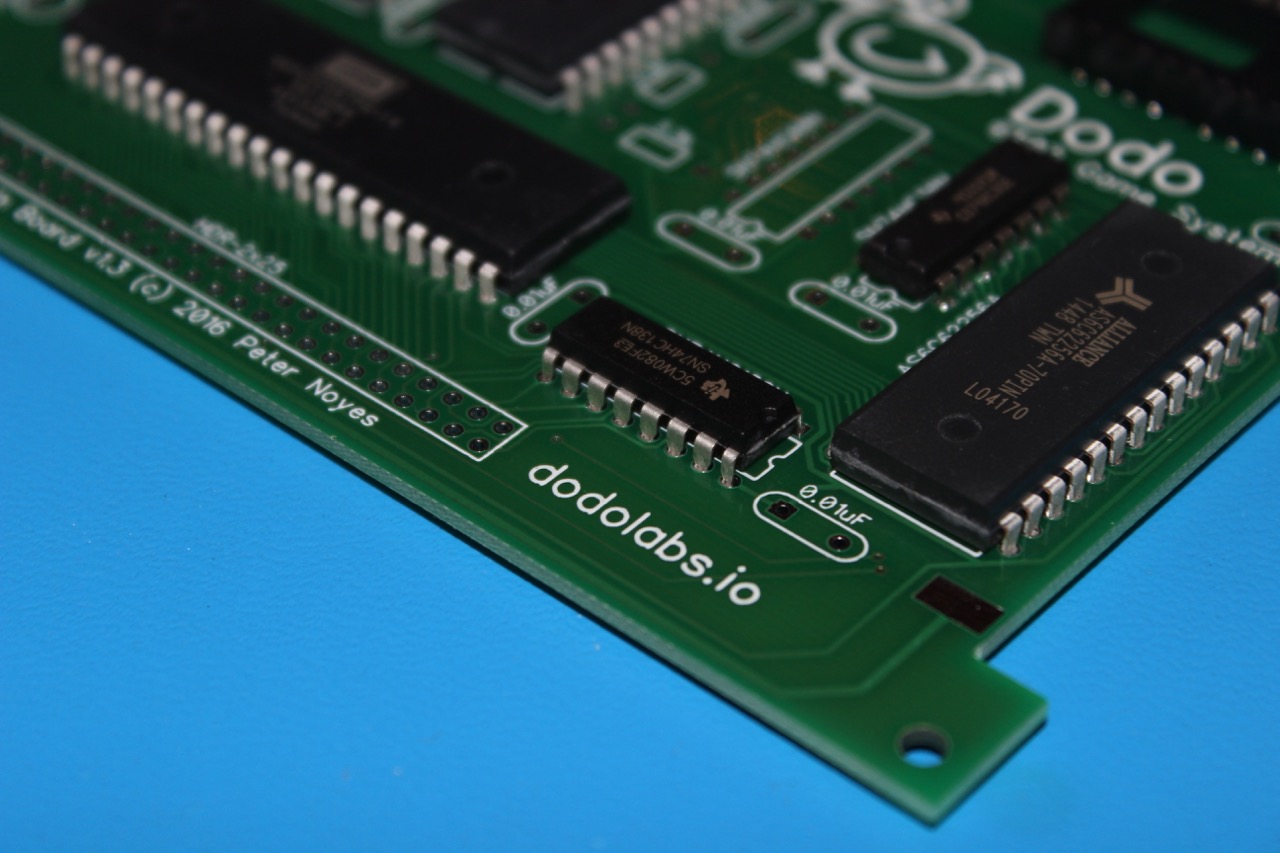
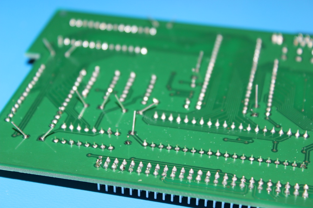
There is no right order to assemble this board as long as all components are installed in the correct orientation. Below is a reasonable order that is not too difficult to manage. The order does not match the functional grouping of components, it goes by short components first followed by taller ones so that when the board is upside down the components are pushed flush against the board. ICs are relatively short, so they are a great place to start. For all of the ICs double check the orientation before soldering.
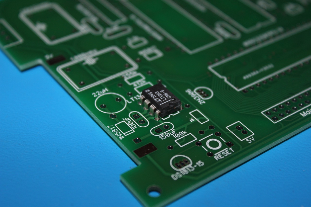
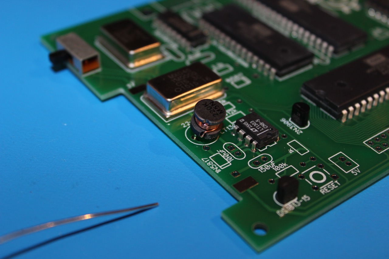
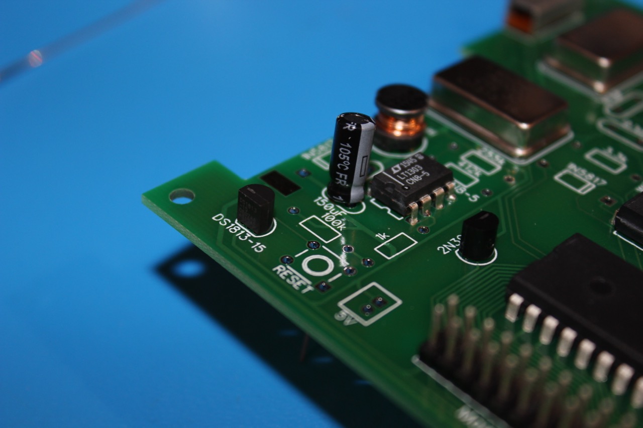
LT1303
The voltage regulator should be done first because it is a tad shorter than the others
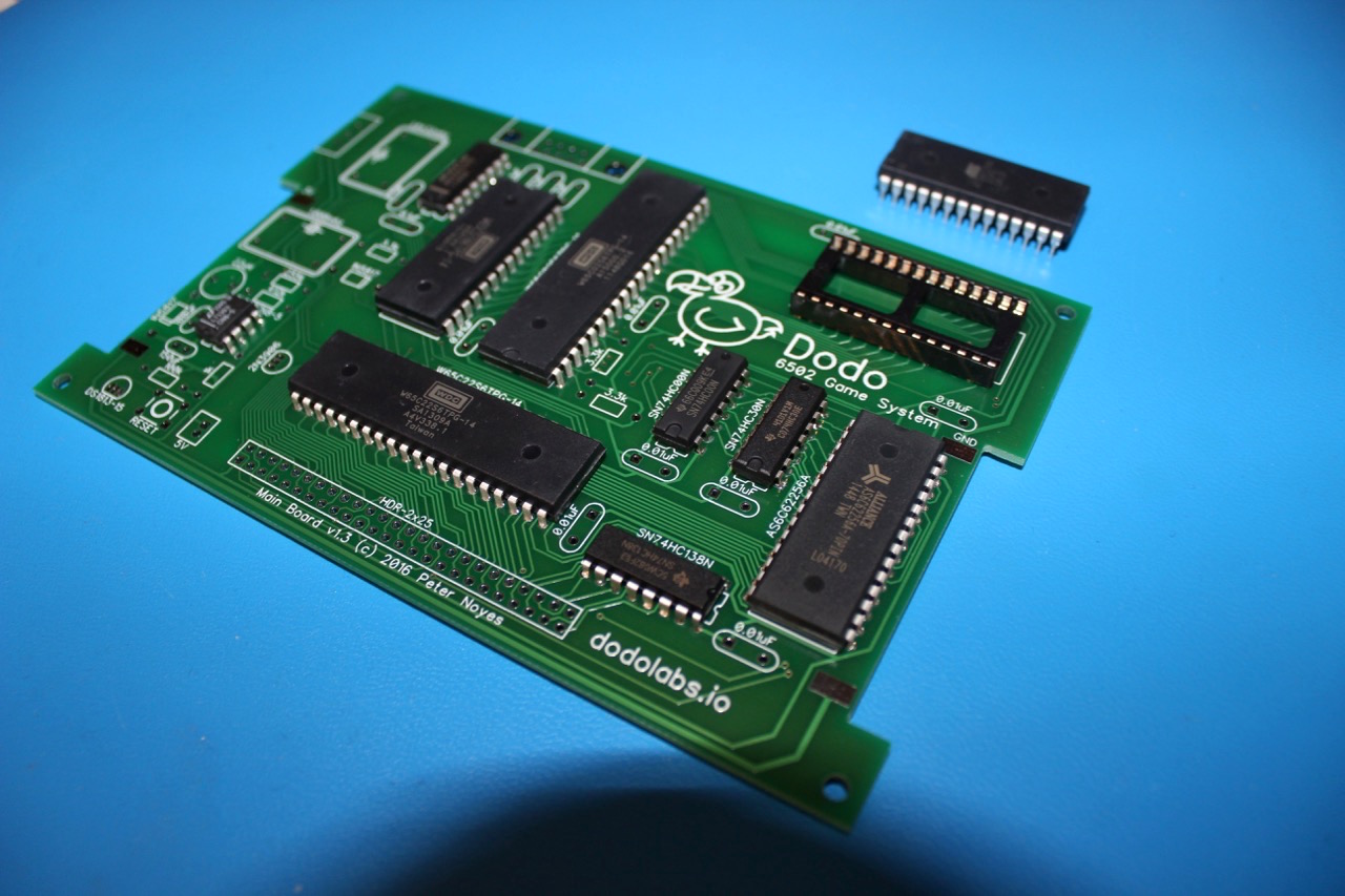
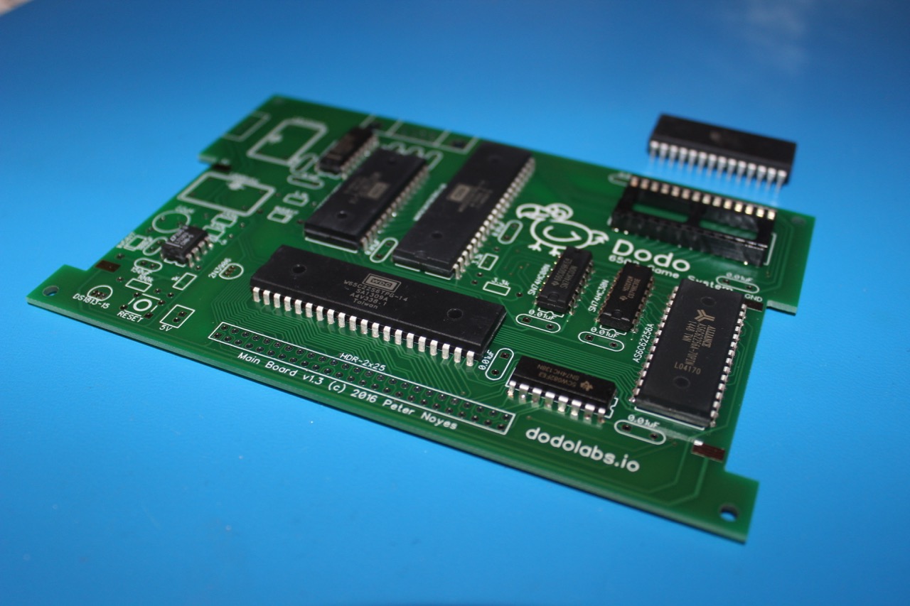
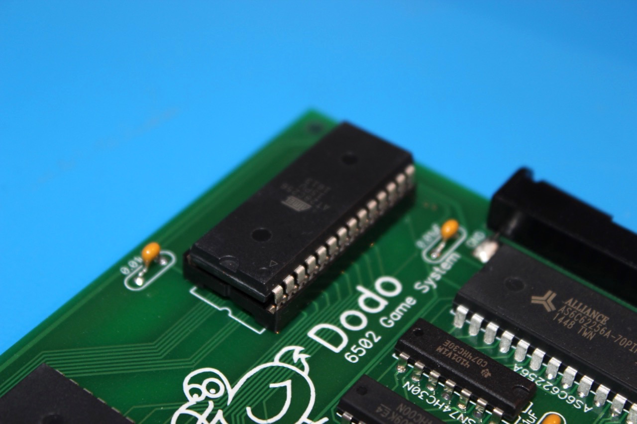
EEPROM Socket
The EEPROM socket should be soldered next. The EEPROM itself is the AT28C256 and can be inserted into the header at a later time.
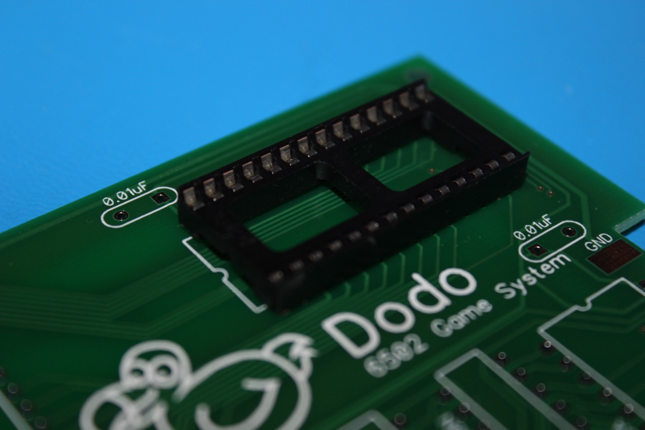
The board will most likely be unstable while doing this. Propping the board with a small item can make soldering easier.
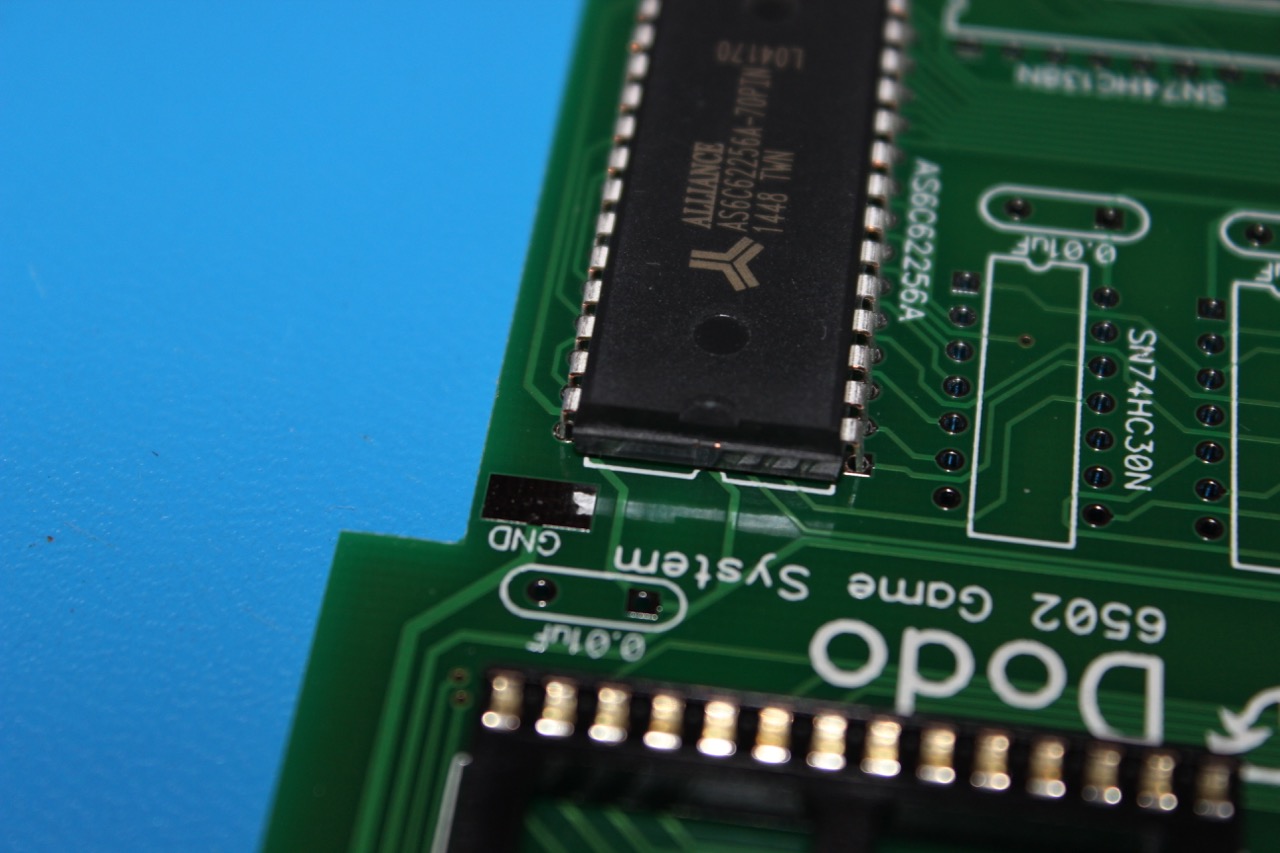
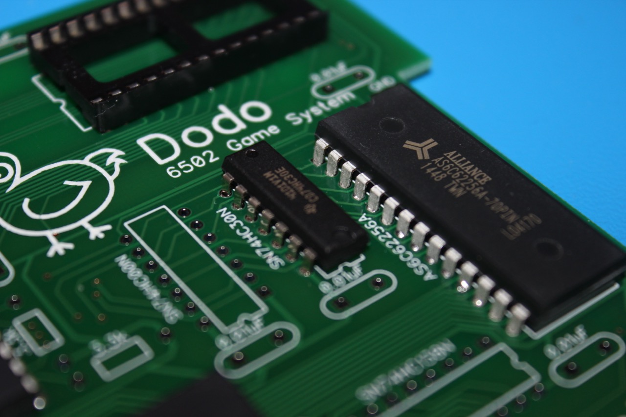
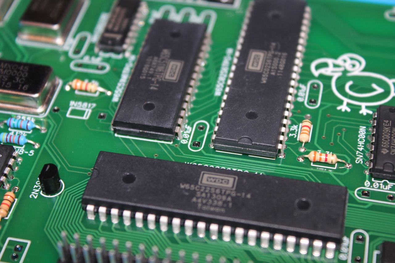
SRAM - AS6C62256A
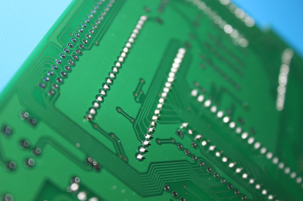
By soldering the SRAM next, the board will now be pretty balanced for soldering the remaining ICs. It can be tricky to insert these larger ICs into the board. The pins need to be bent slightly inward before inserting, and it may take even more bending while simultaneously gently pushing the IC into the holes.
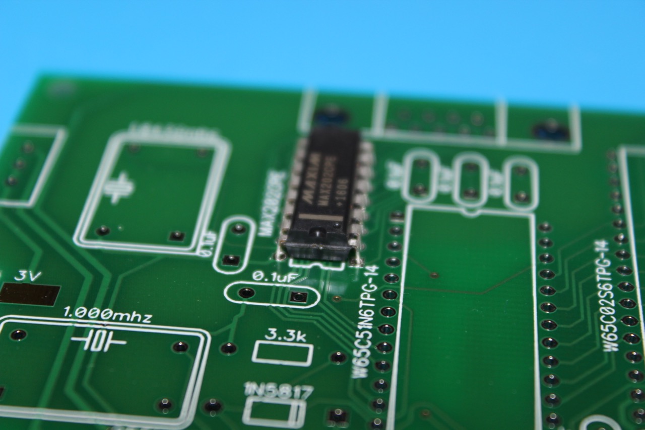
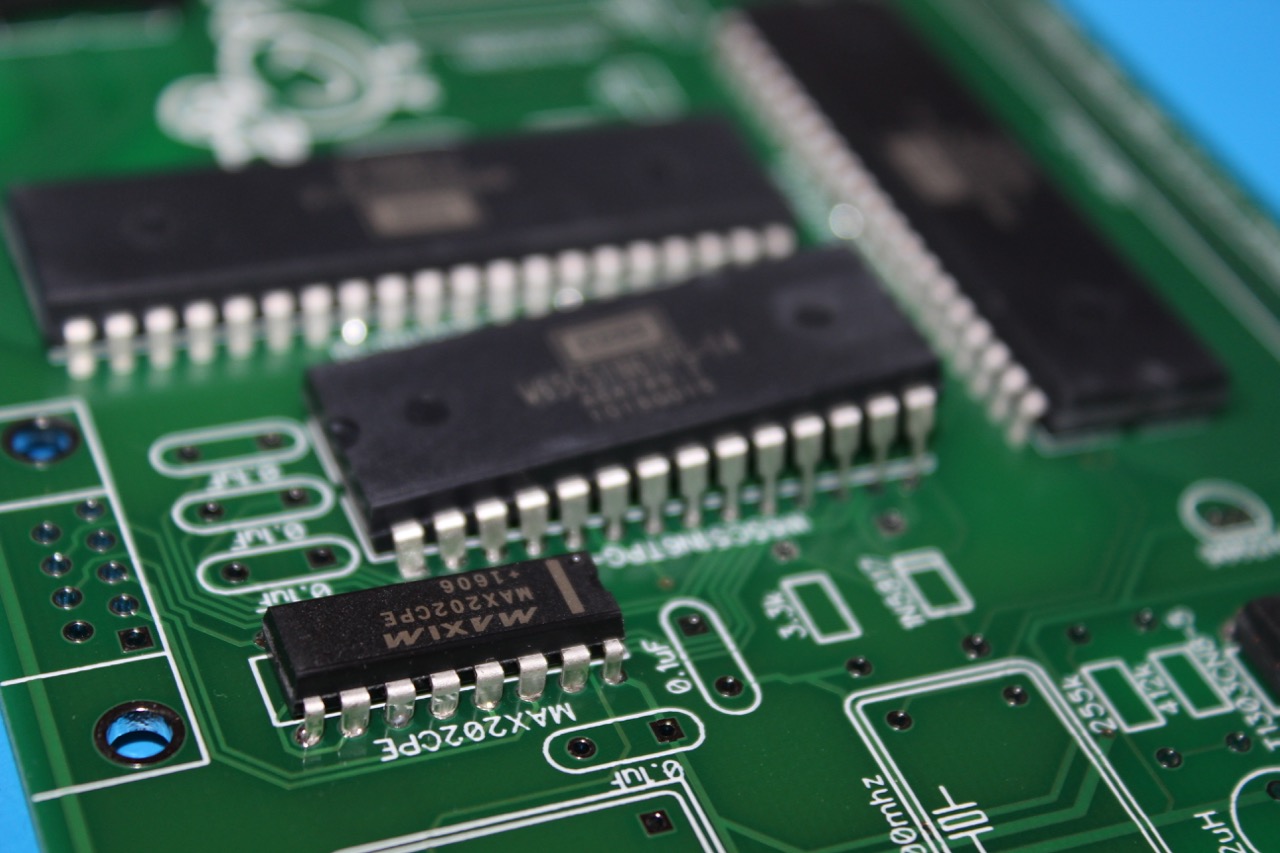
MAX202CPE - RS-232 Interface
65C02 - Processor
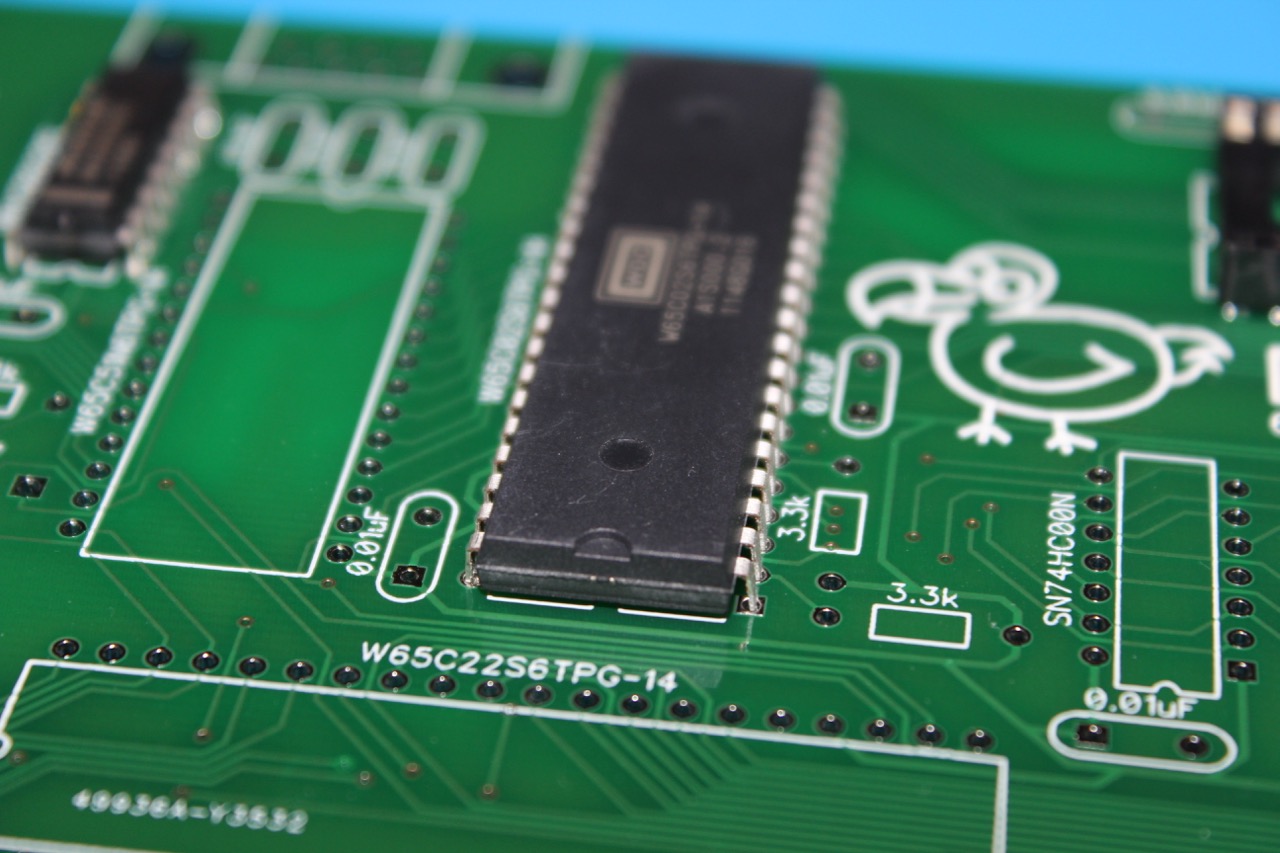
65C22S - Peripherial Adapter
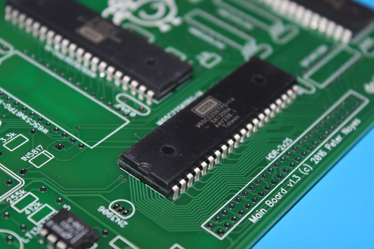
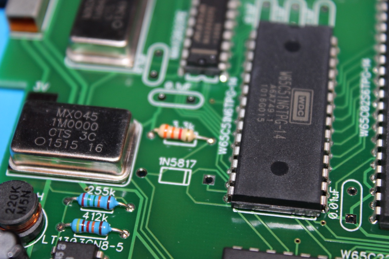
65C51 - Communication Adapter
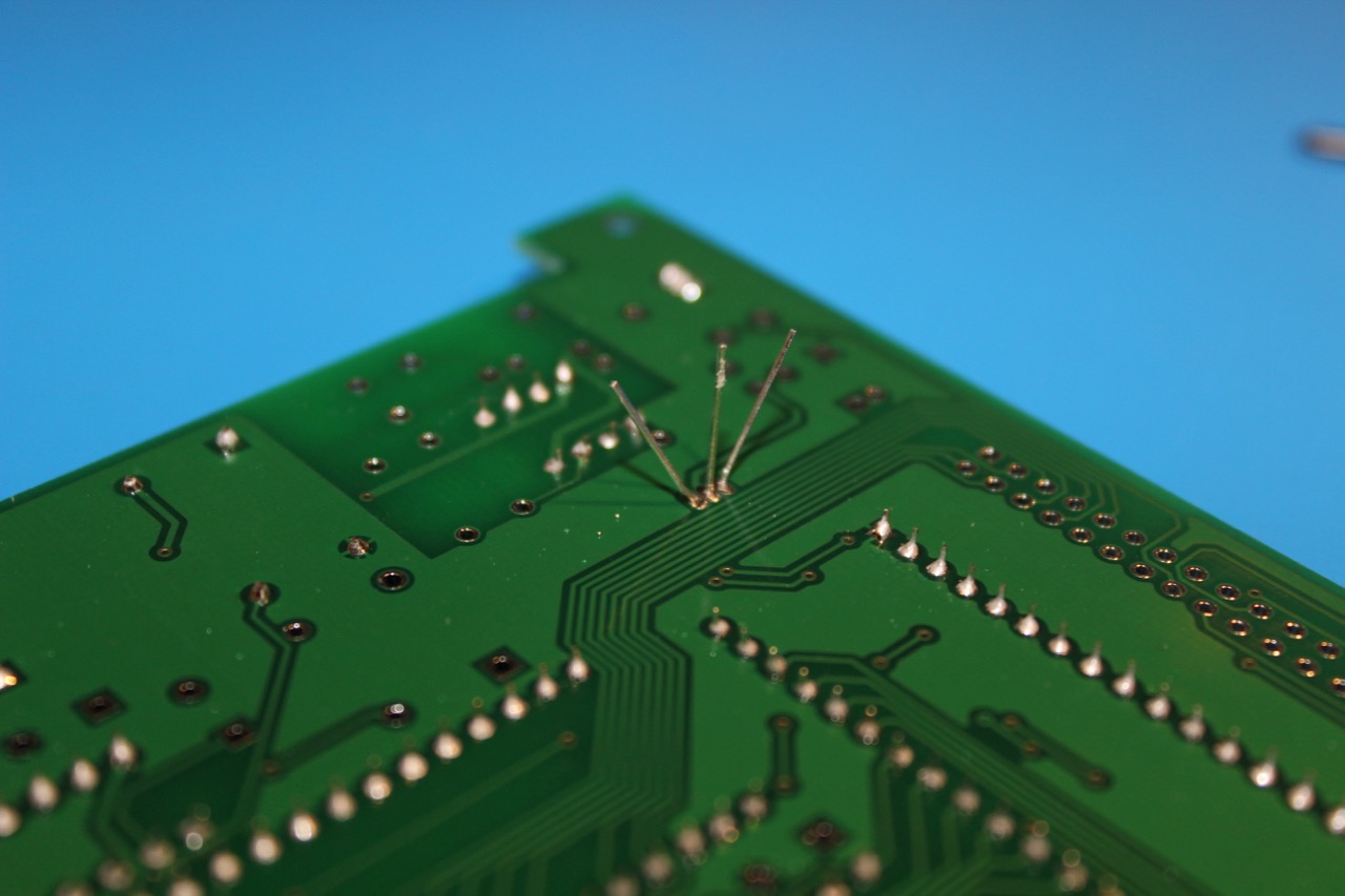
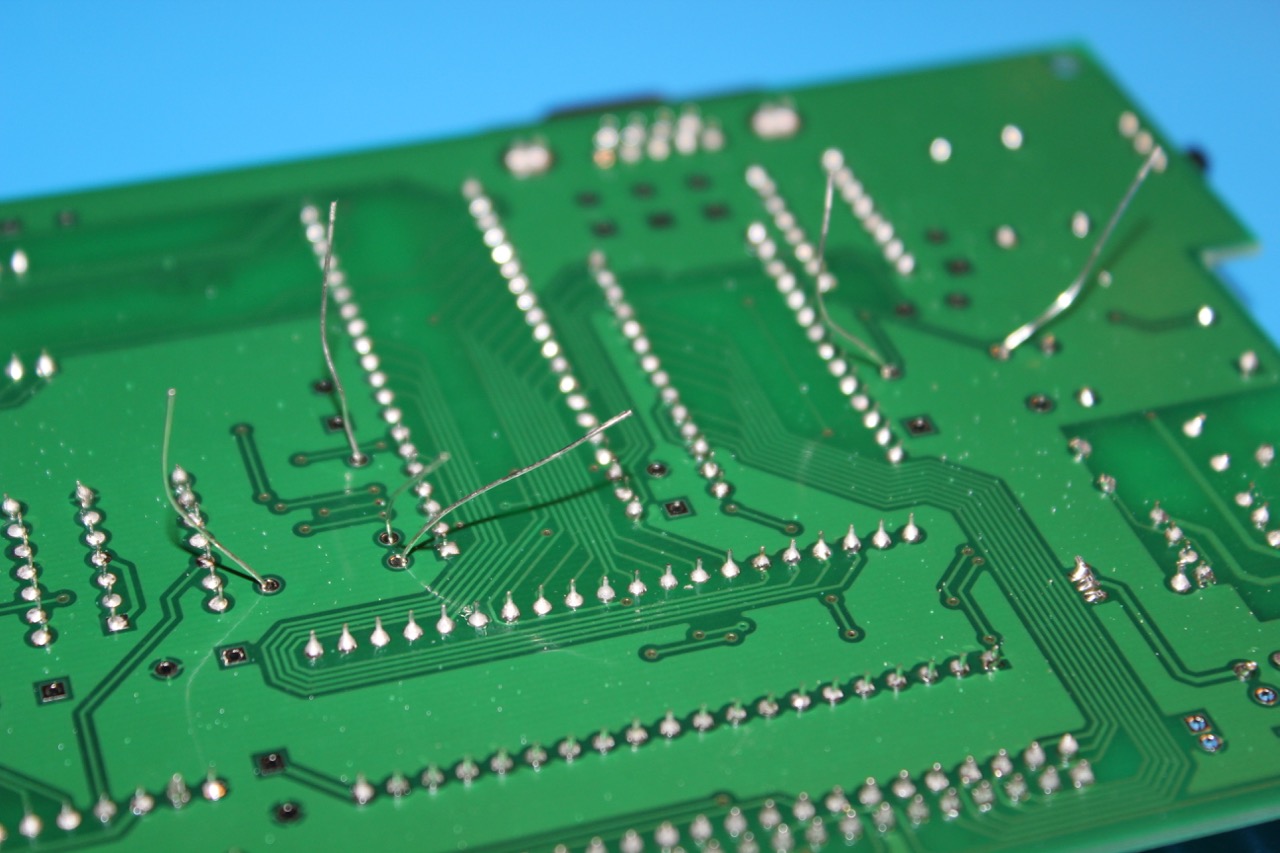
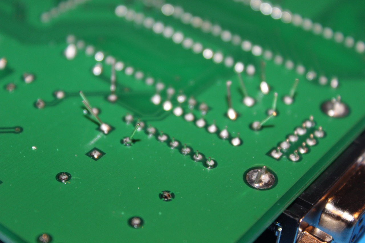
Below shows inserting a chip from one side. At this point gently bend then pins inward while working the rest of the chip into the holes.
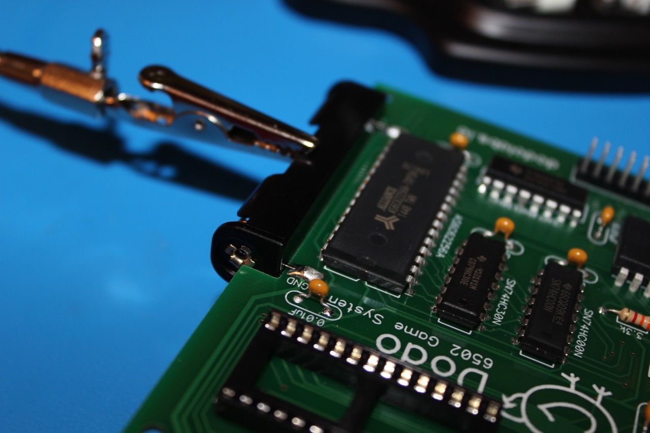
74HC30 - 8 input NAND gate
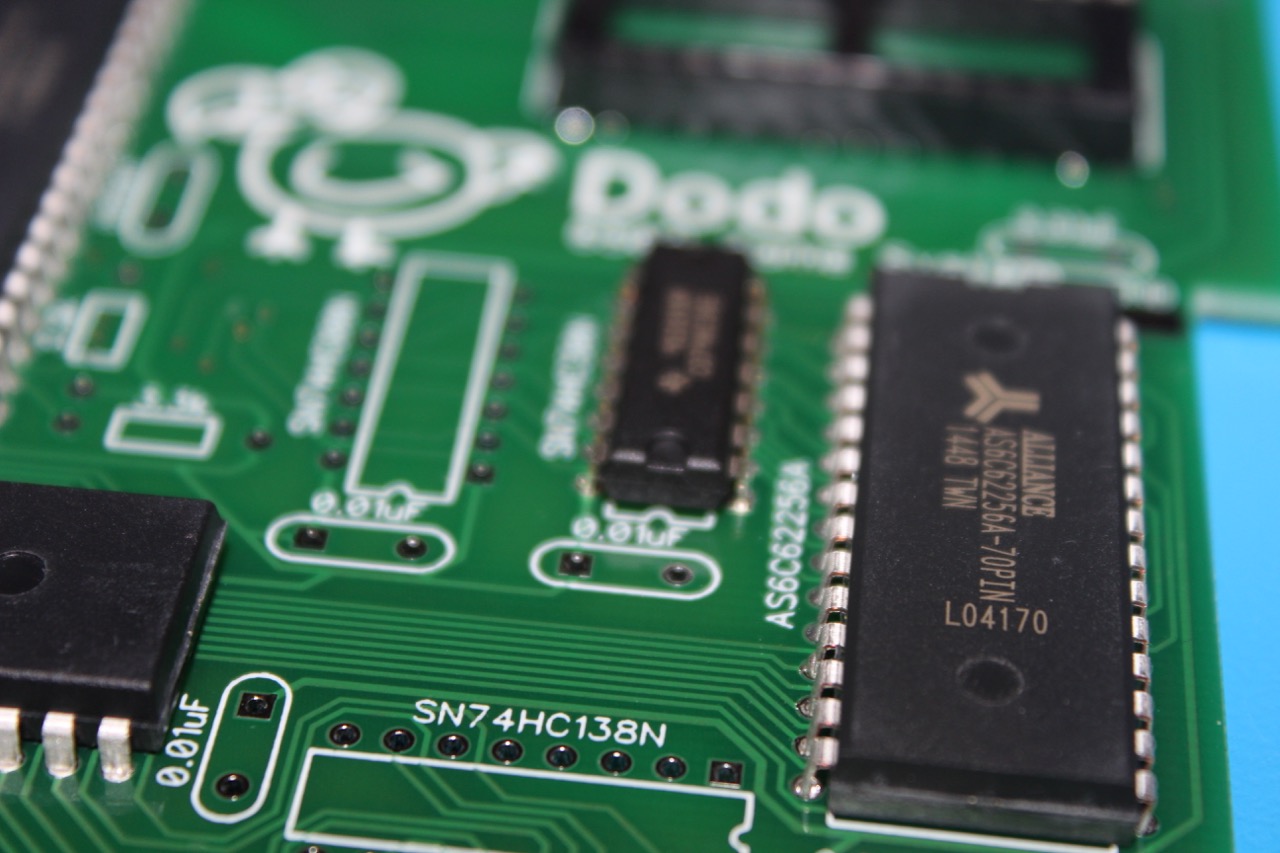
74HC138 - 3 to 8 Decoder
74HC00 - Quad 2 input NAND gate
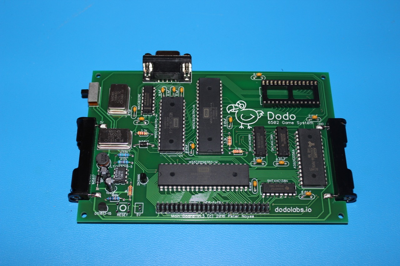
ICs are Complete
All of the ICs should now be in place!
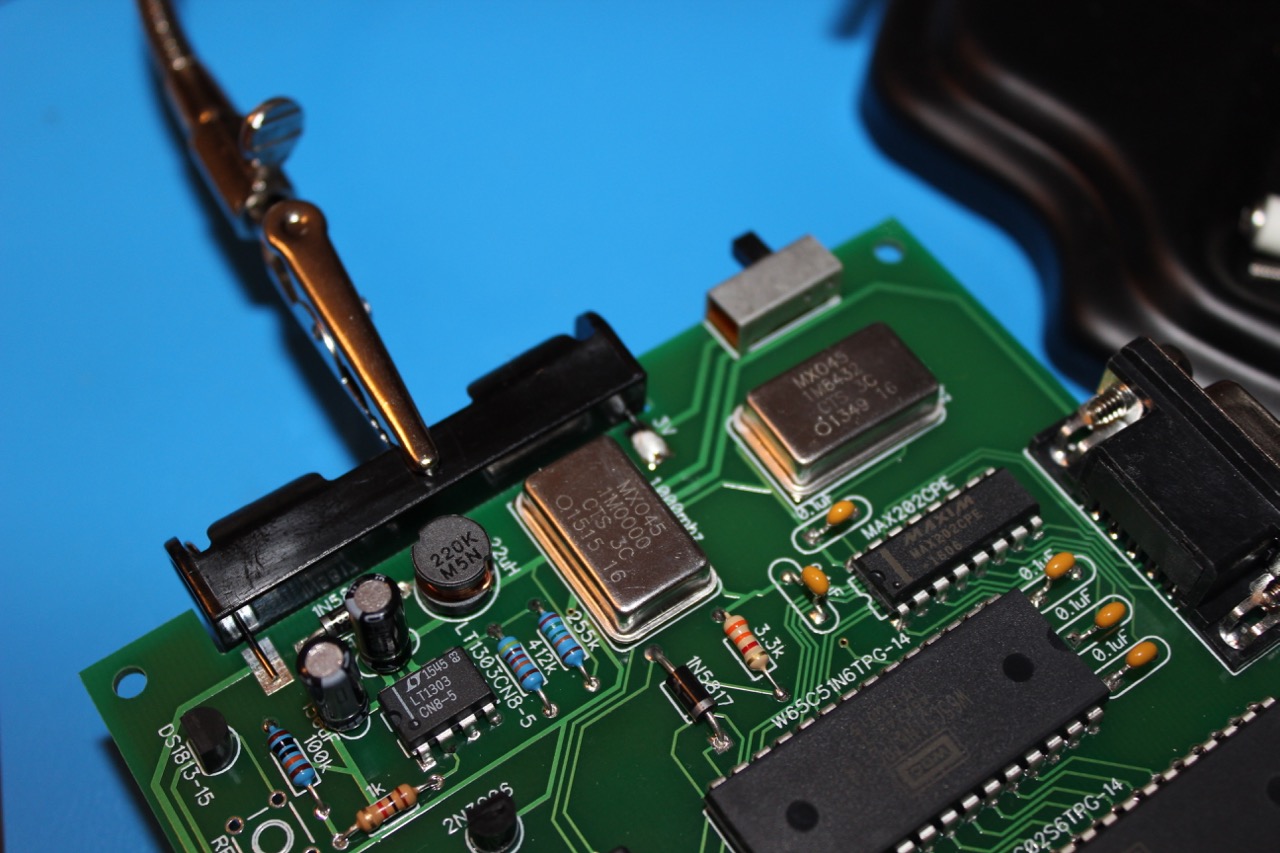
Step 2 - Oscillators
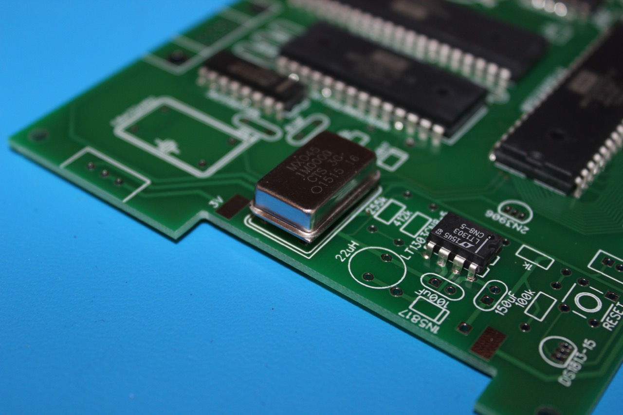
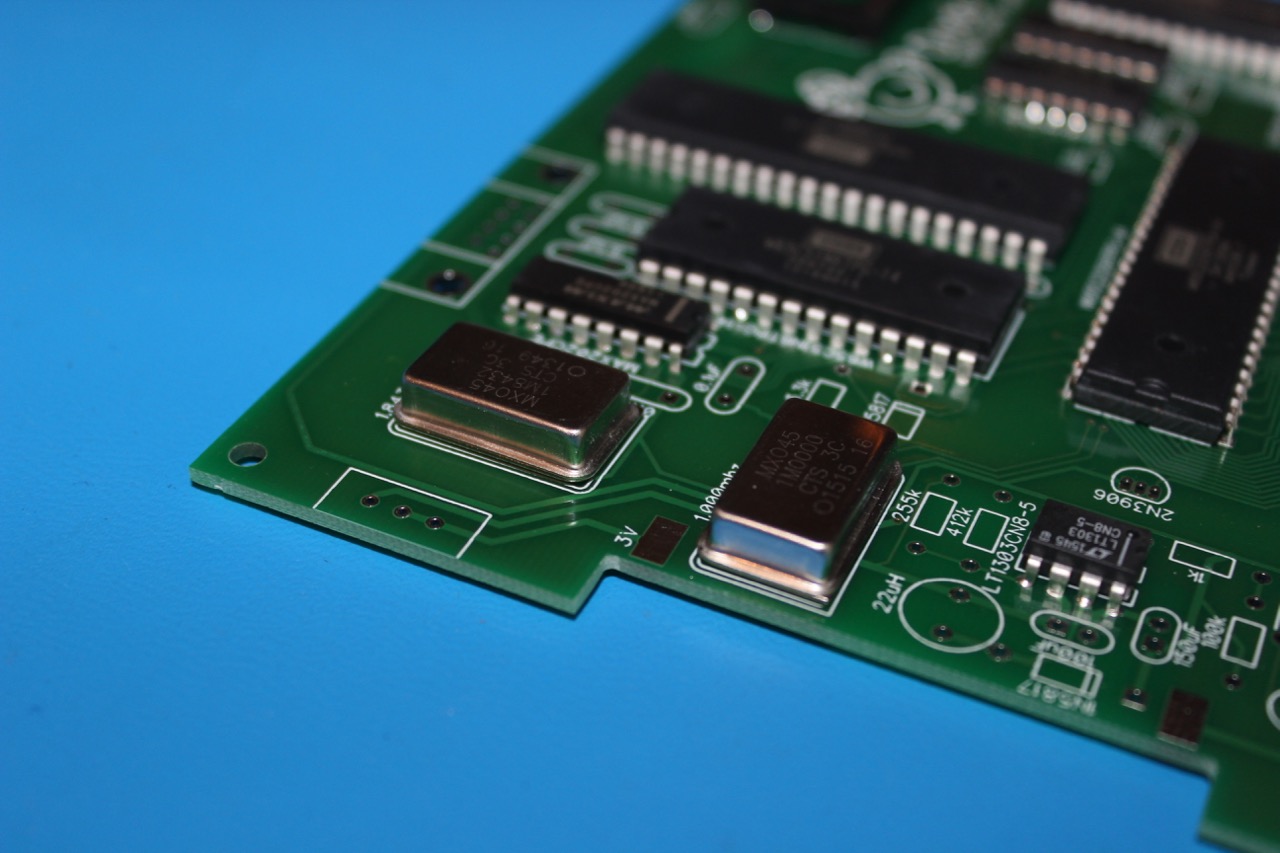
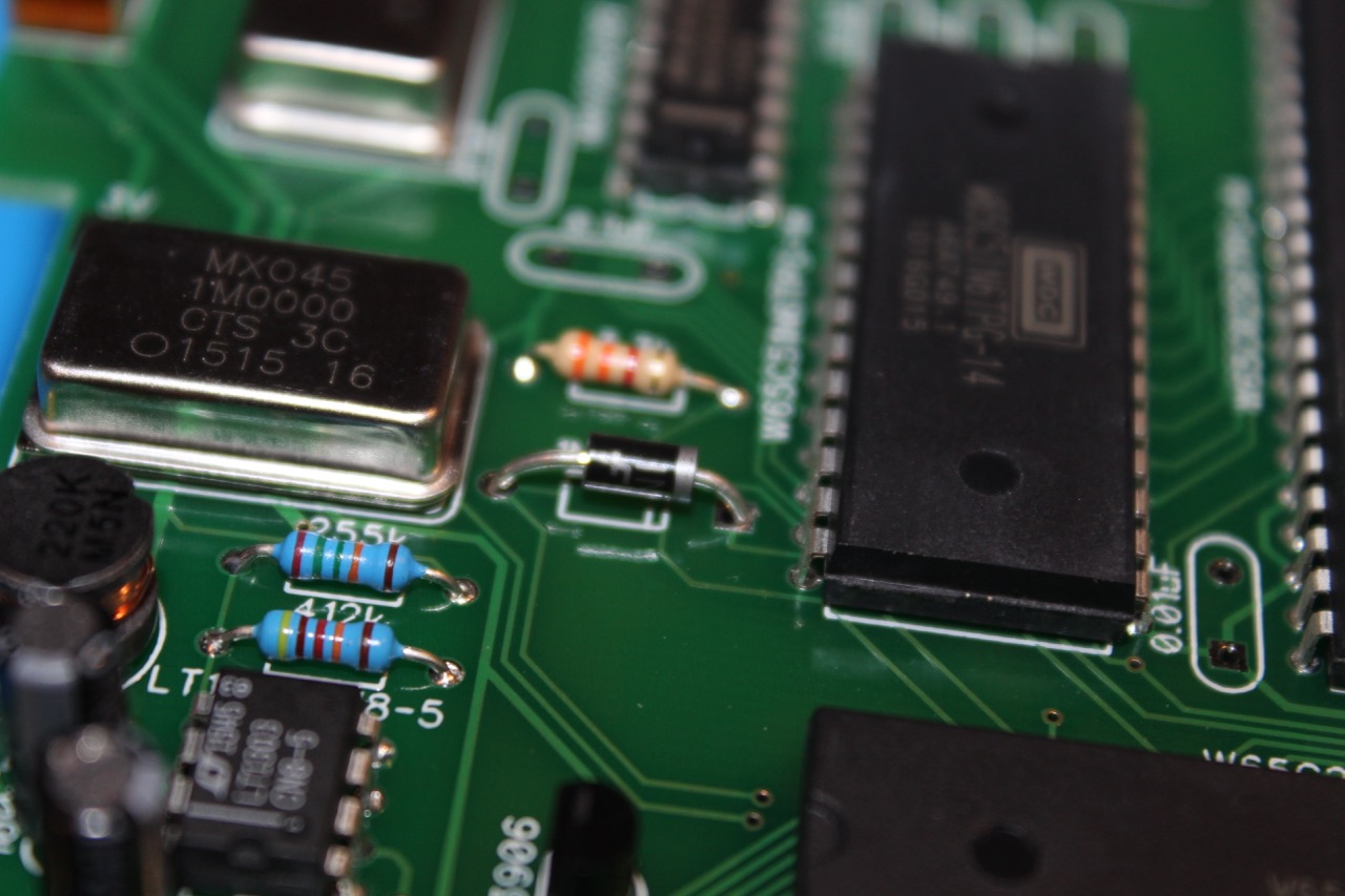
1.000mhz Oscillator - Main clock
The oscillators need to be installed in the correct orientation. 3 of the corners are rounded and 1 is square. The square corner needs to be aligned with the square corner on the PCB’s silkscreen.
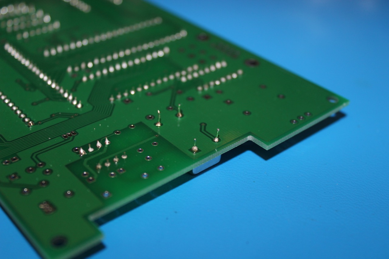
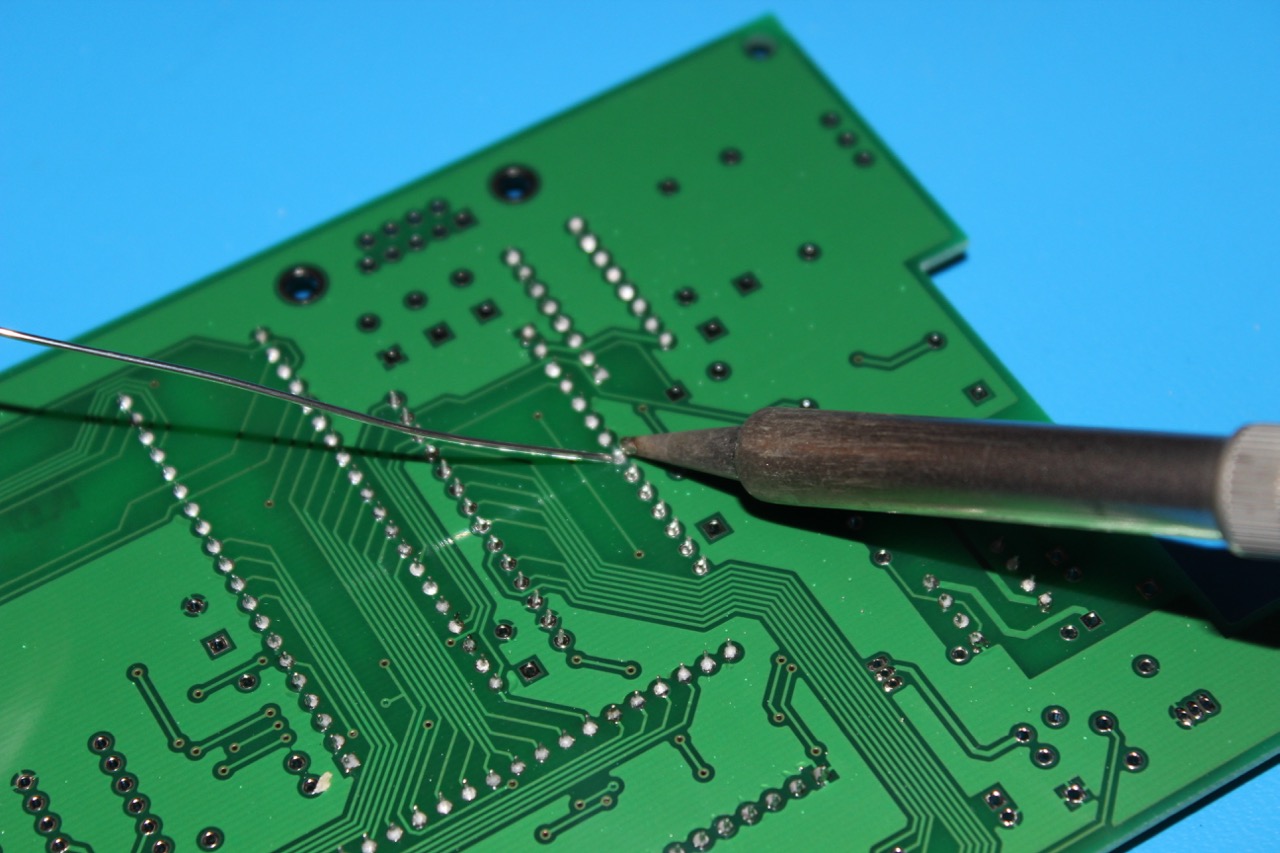
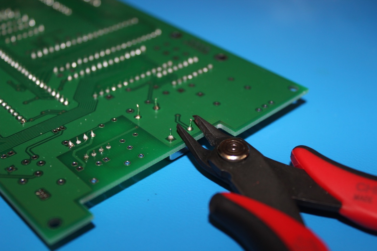
For the first time, leads need to be trimmed. Flush wire cutters work best.
1.8432mhz Oscillator - Clock for the baud generator in the 65C51
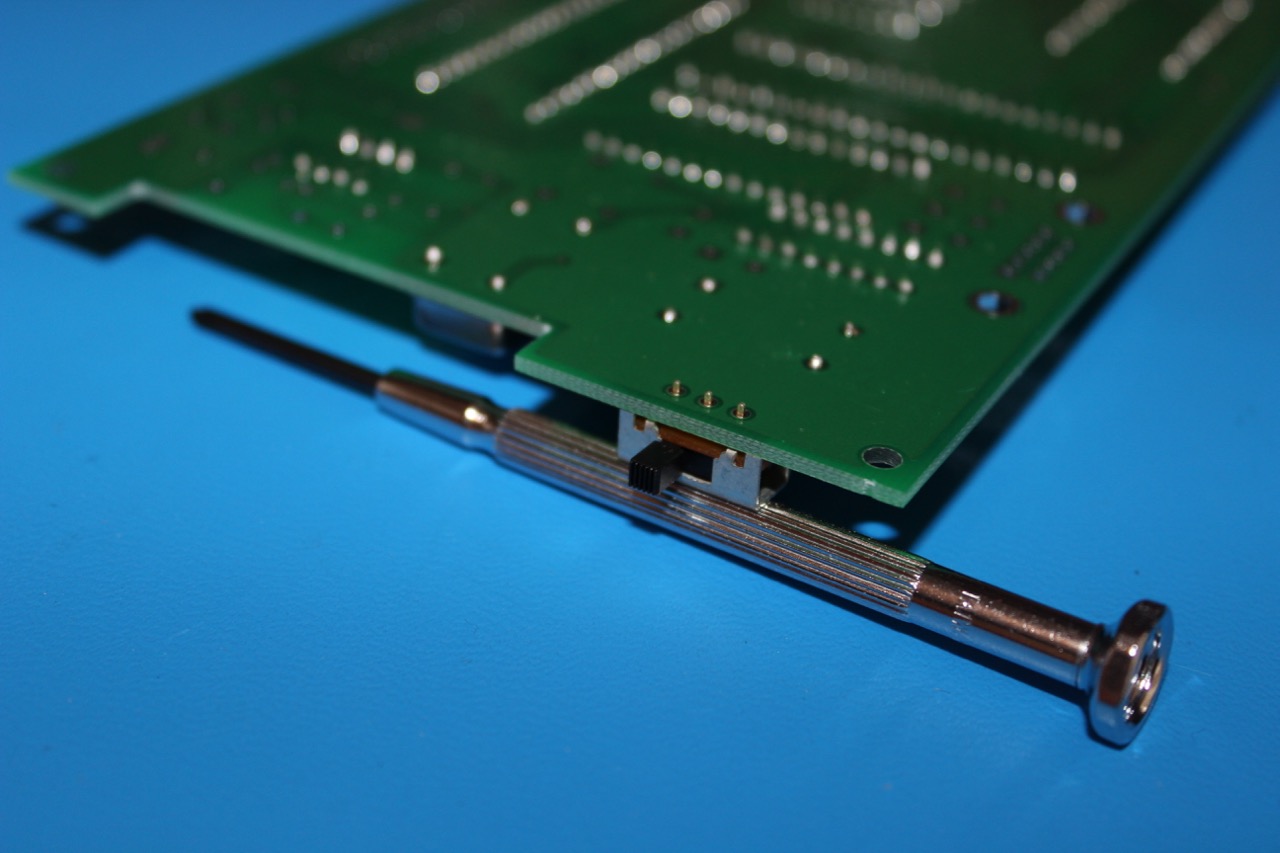
Step 3 - Switch
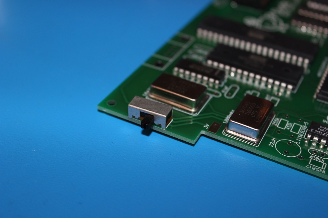
To make sure the switch is flush against the board, it may need to be propped up.
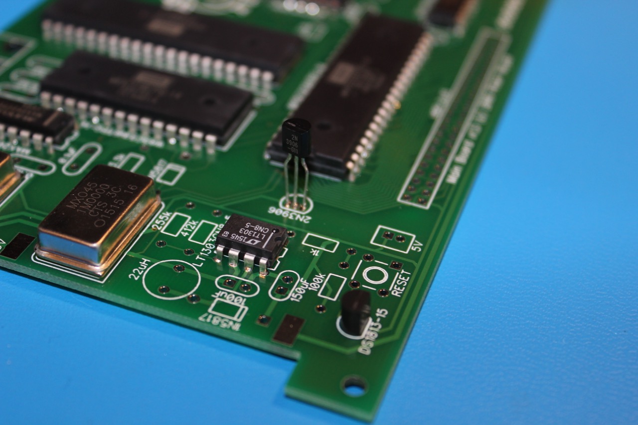
Step 4 - TO-92 components
Be careful not to cause any bridges when soldering these components. The leads are spaced pretty close to each other. If you have a multimeter it might be worthfile double checking that there are no shorts. Also, these components look very similar, and there are an additional 2 TO-92 components on the I/O Board. Double check that the correct component is being installed.
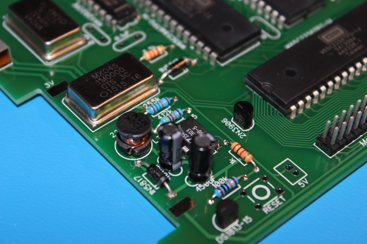
DS1813 - Reset Package
2N3906 - PNP Transistor for driving Low Battery LED
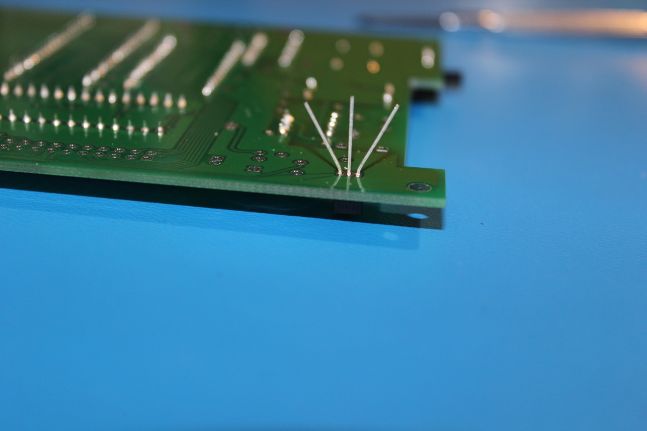
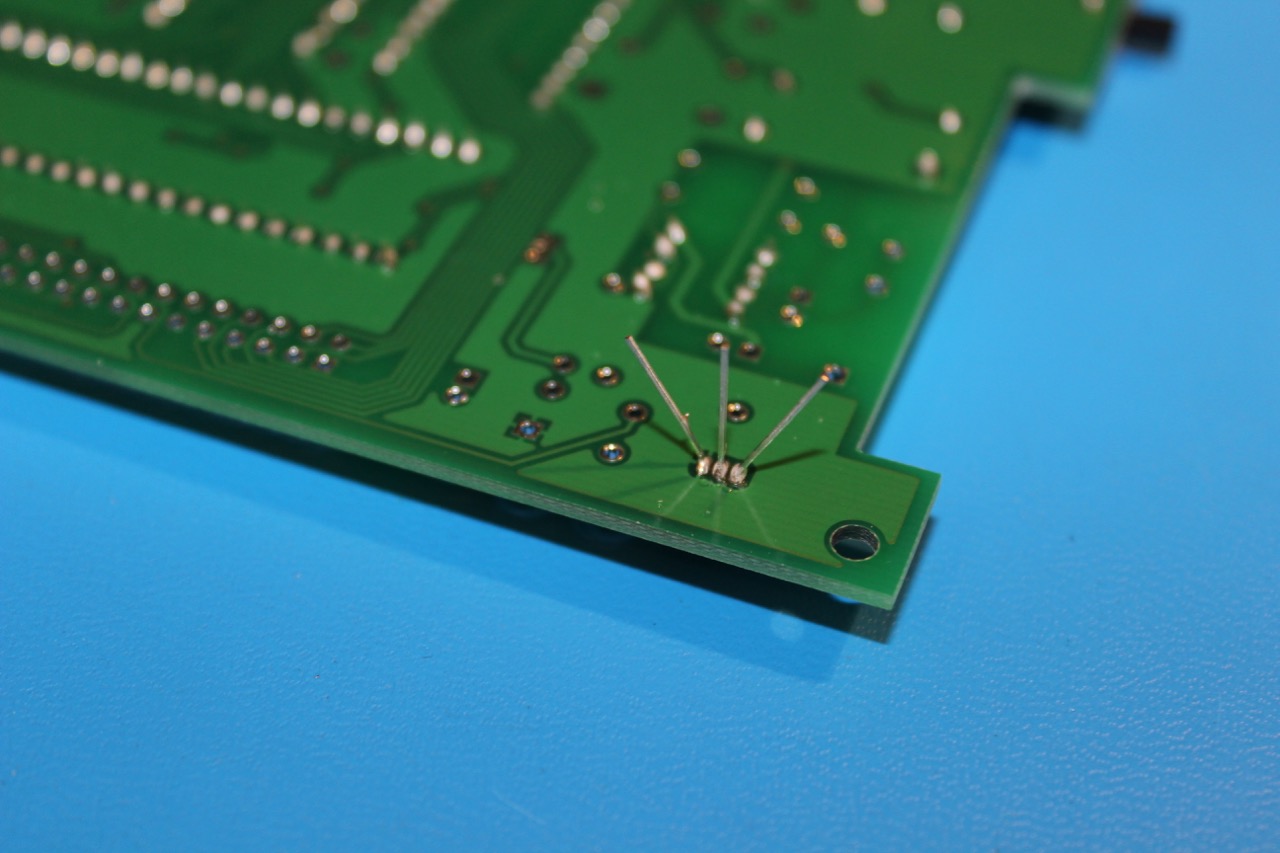
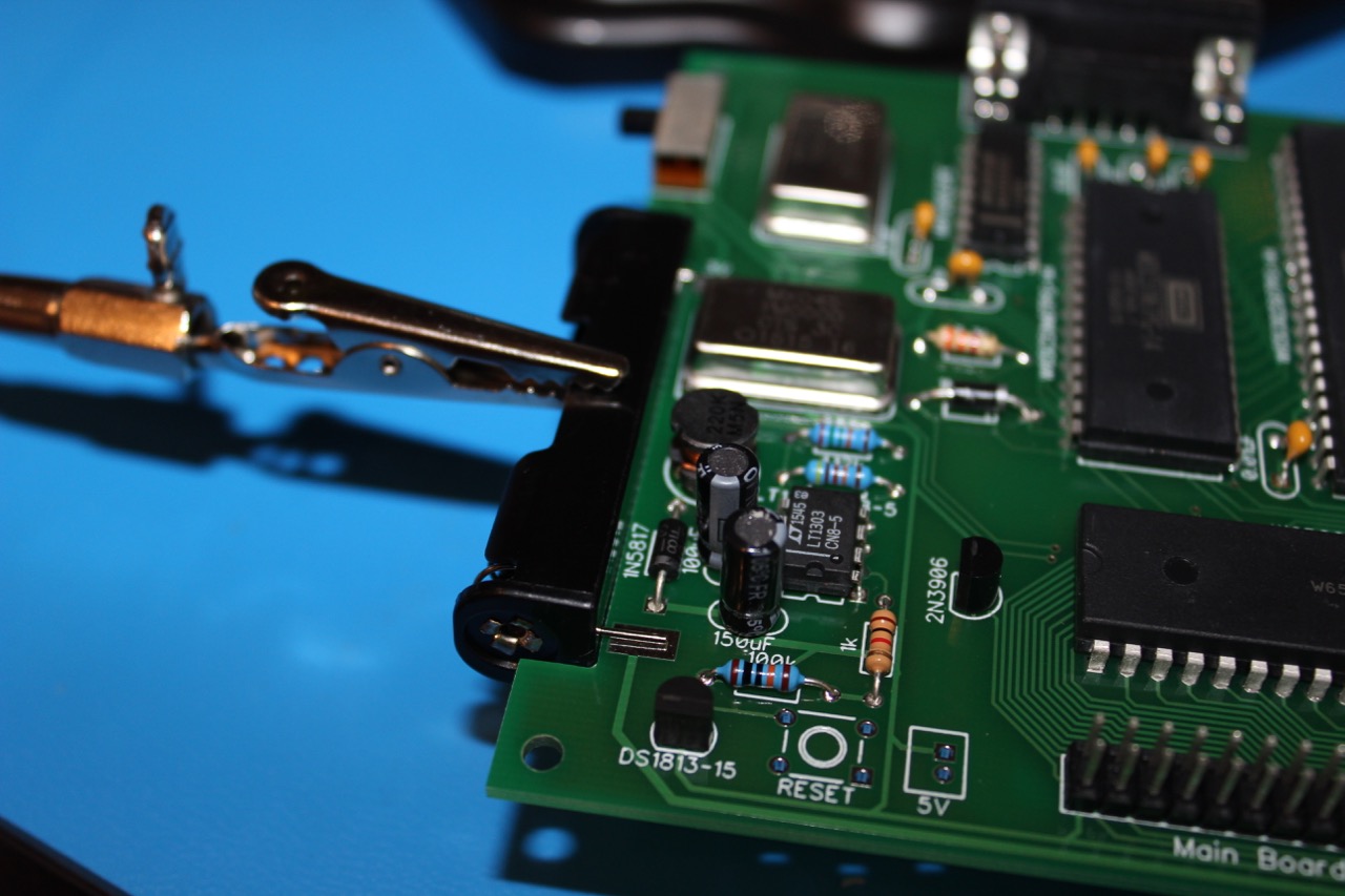
Step 5 - Inductor
The inductor is not polarized
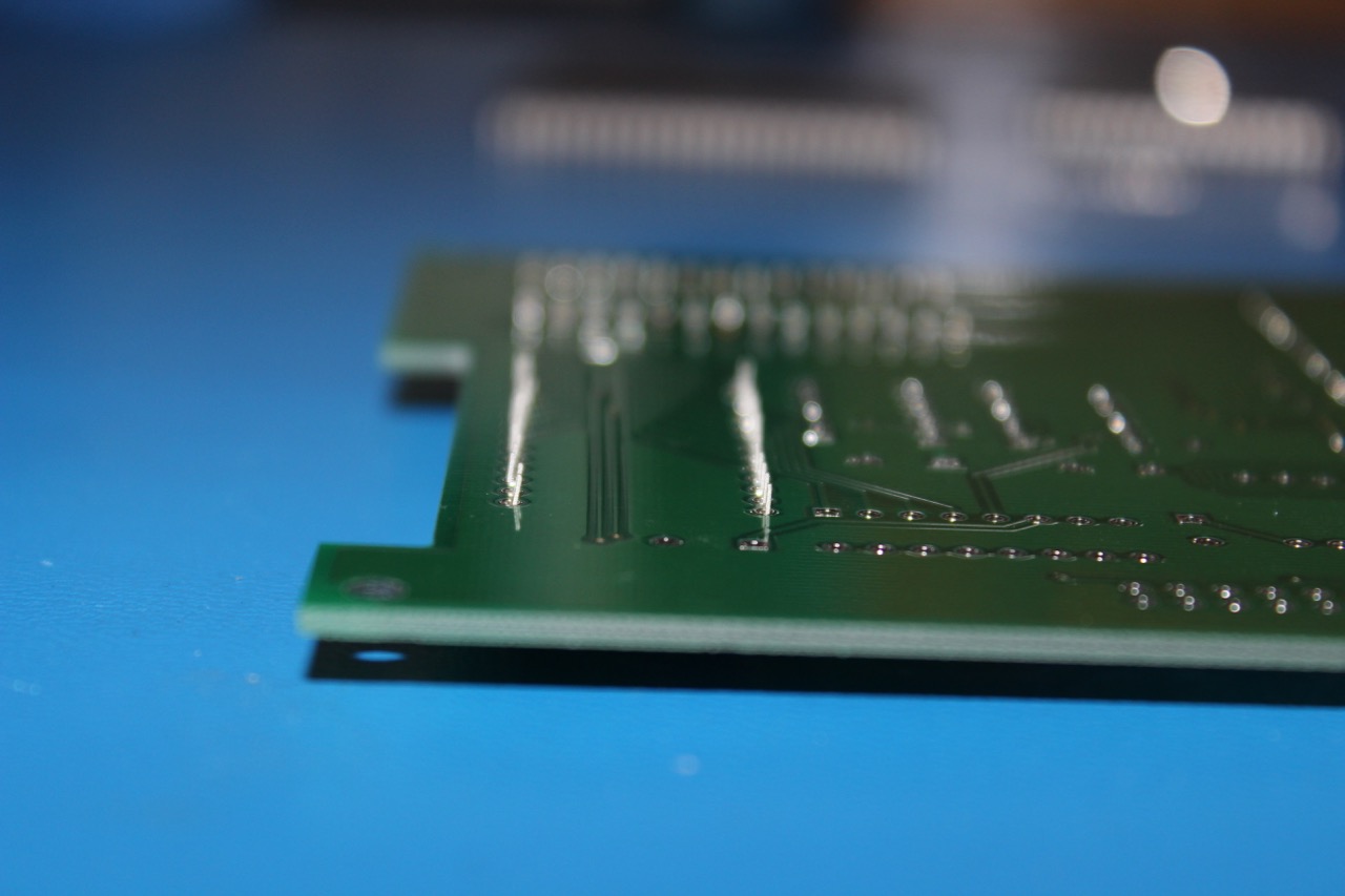
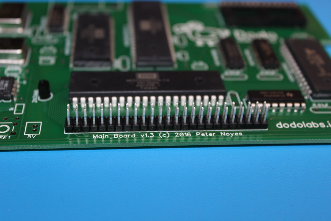
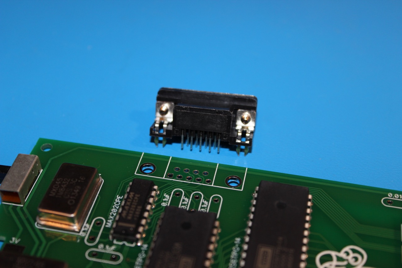
Step 6 - Header
It is best to use the male header for the main board so that logic analyzer probes could be easily hooked up
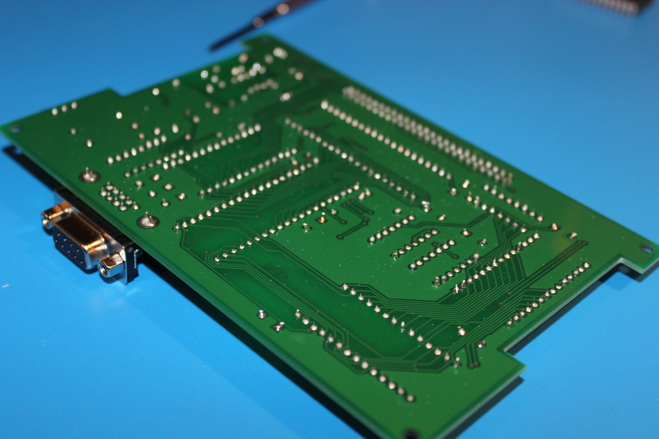
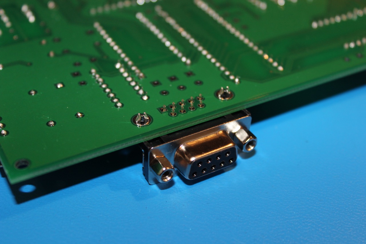
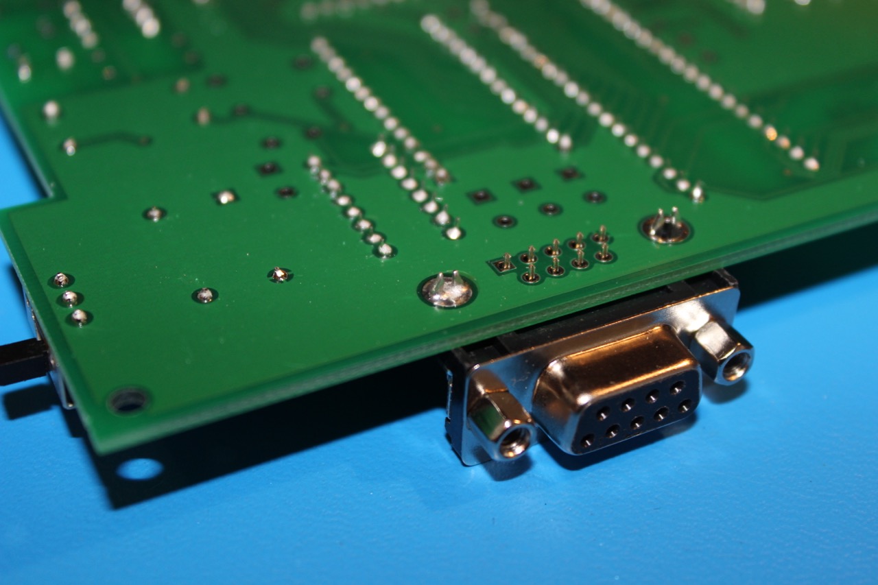
Step 7 - DB9 Connector
There are two large holes for the DB9 clips to hold it in place. These require a large amount of solder. To solder, move the iron and solder around to different sides of the hole to ensure it completely fills with solder.
Step 8 - Electrolytic Capacitors
The electrolytic capacitors are polarized. The ground lead goes into the round hole. The positive lead goes into the square hole. Note that the capicitors look nearly identical but one is 100uF and one is 150uF.
150uF
100uF
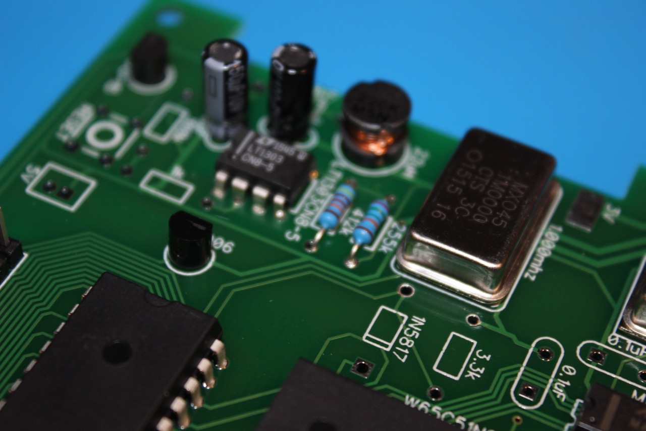
Step 9 - Resistors
255k
The 255k resistor is: RED GREEN GREEN ORANGE
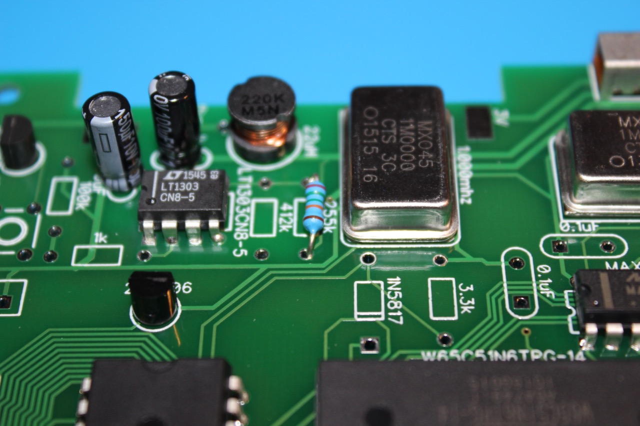
412k
The 412k resistor is: YELLOW PURPLE RED ORANGE
100k
The 100k resistor is: BROWN BLACK YELLOW
1k
The 1k resistor is: BROWN BLACK RED
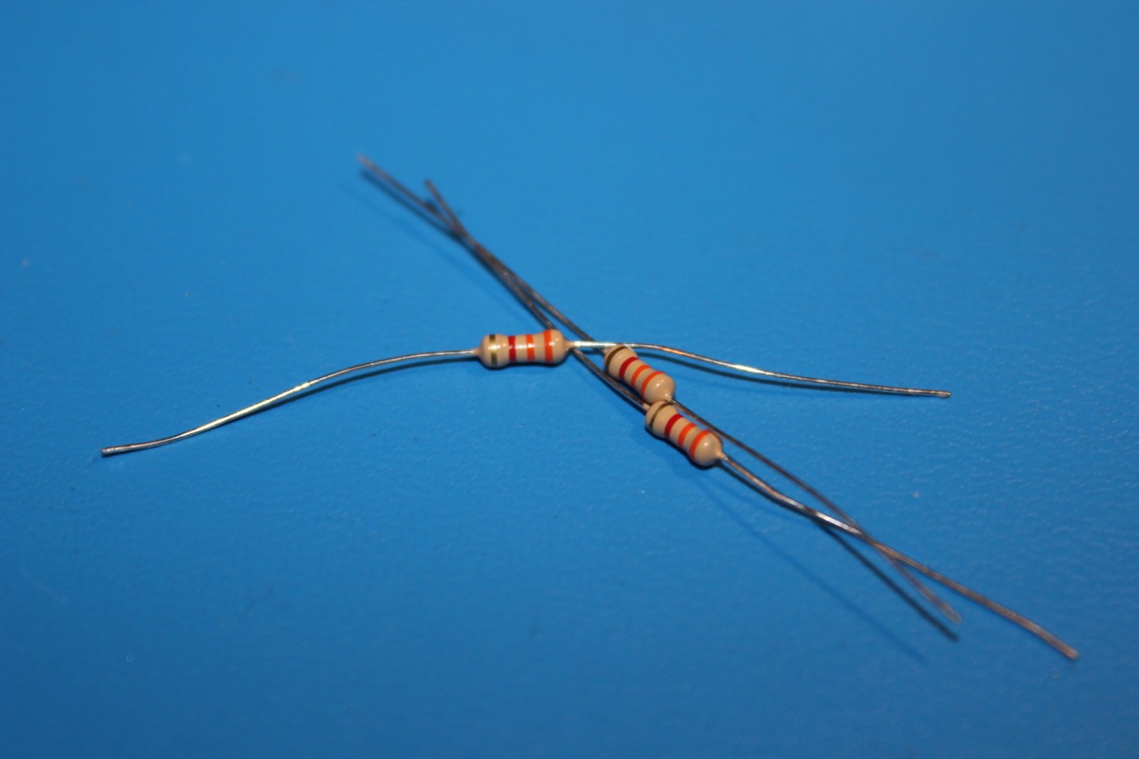
3.3k
There are 3 3.3k resistors and they are: ORANGE ORANGE RED
Step 10 - Diodes
The Diodes are polarized. There is a line on one side of the diode that matches a line on the PCB silkscreen.
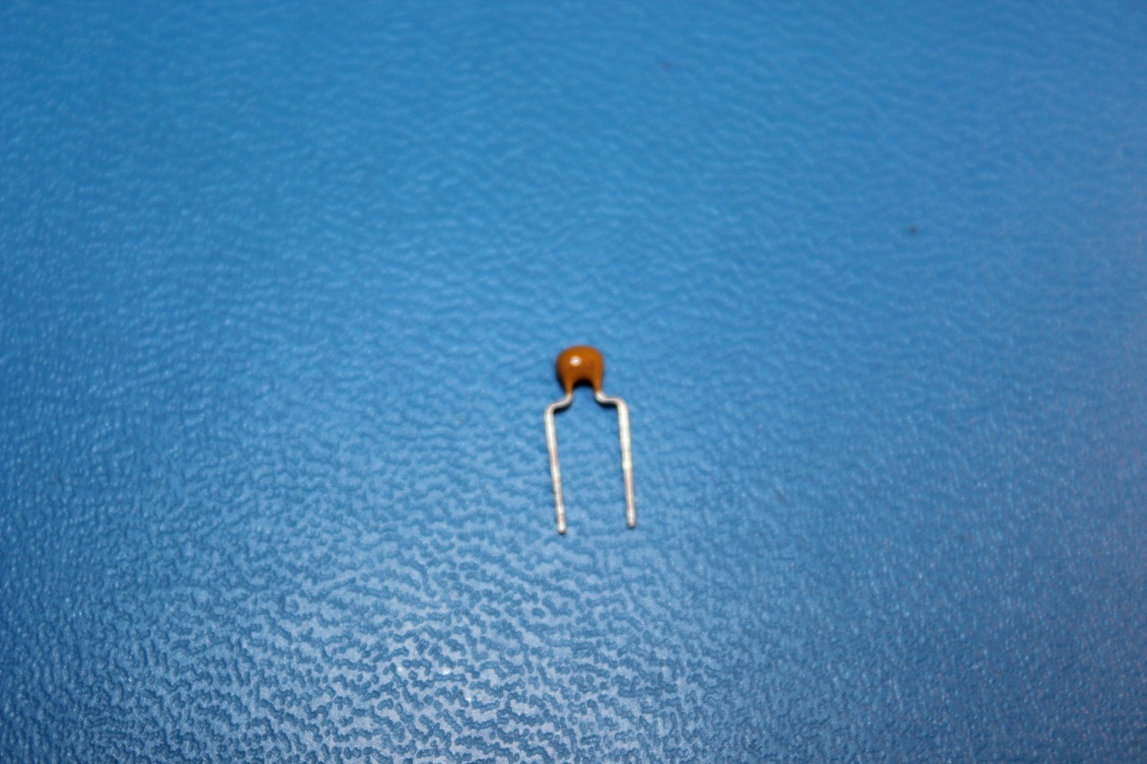
Step 11 - Ceramic Capictors
The ceramic capacitors are not polarized, it doesn’t matter the orientation that they are installed. There are both 0.1uF capacitors and 0.01uF capacitors. There are 5 0.1uF and they are all installed in the vicinity of the MAX202CPE IC. The 0.1uF have the number 104 printed on them. There are 8 0.01uF bypass capacitors that are installed next to each IC. They have 103 printed on them.
0.1uF
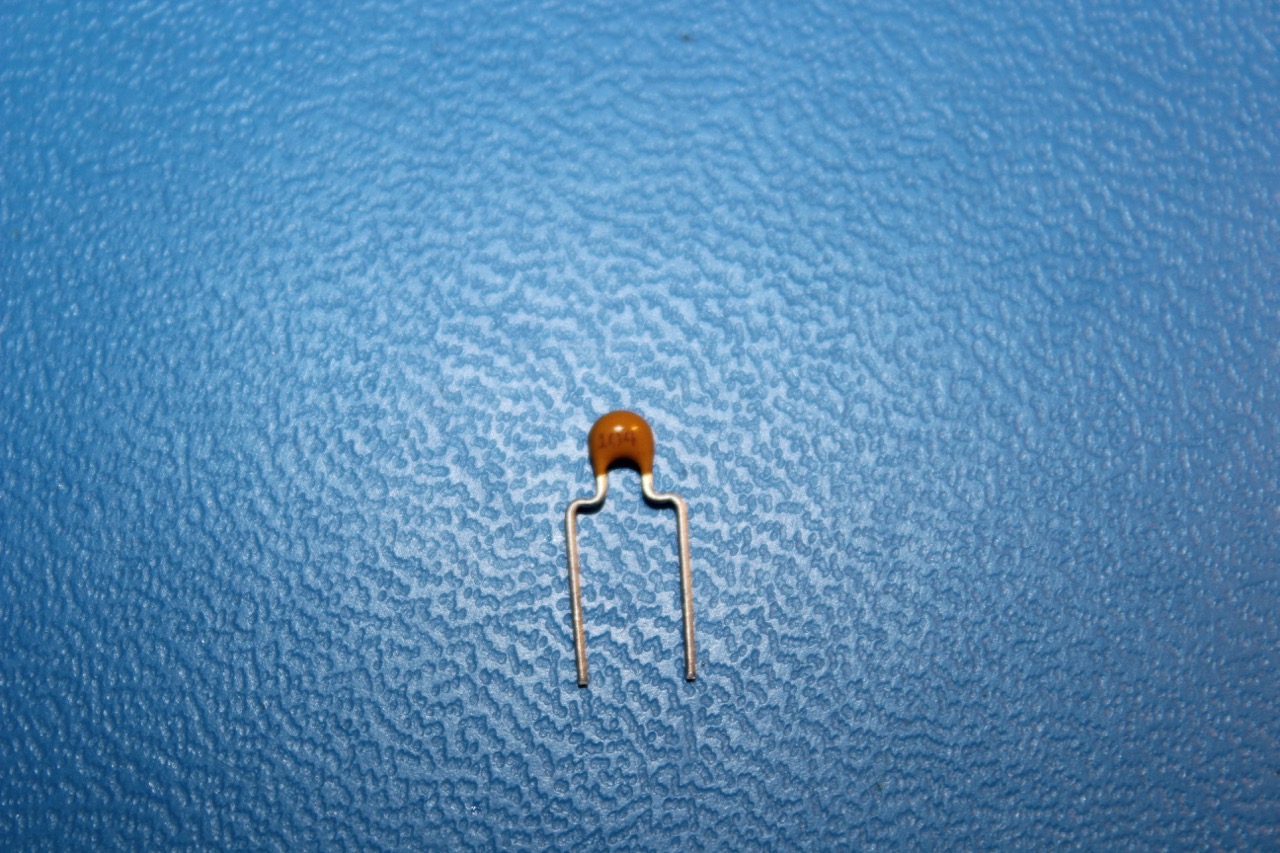
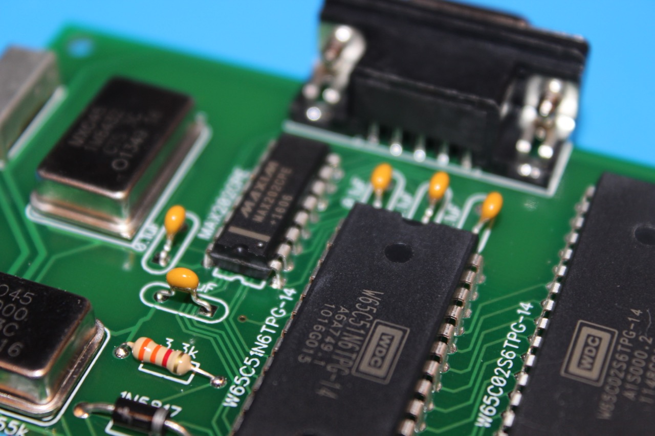
0.01uF
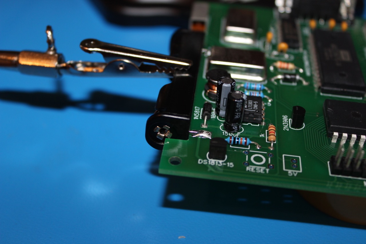
Step 12 - Battery Holders
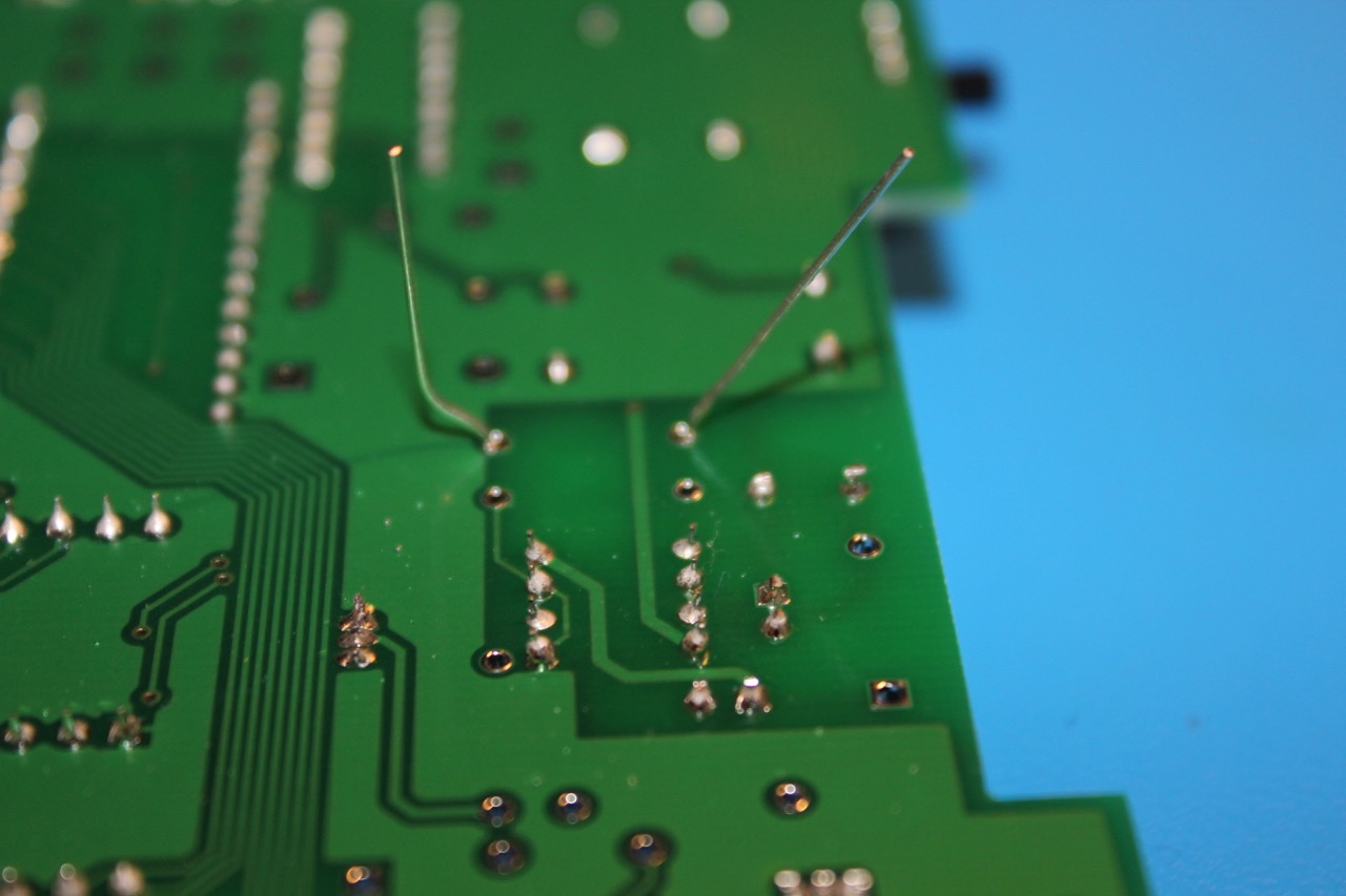
The battery holders are the trickiest part of building Dodo. First, the leads need to be trimmed.
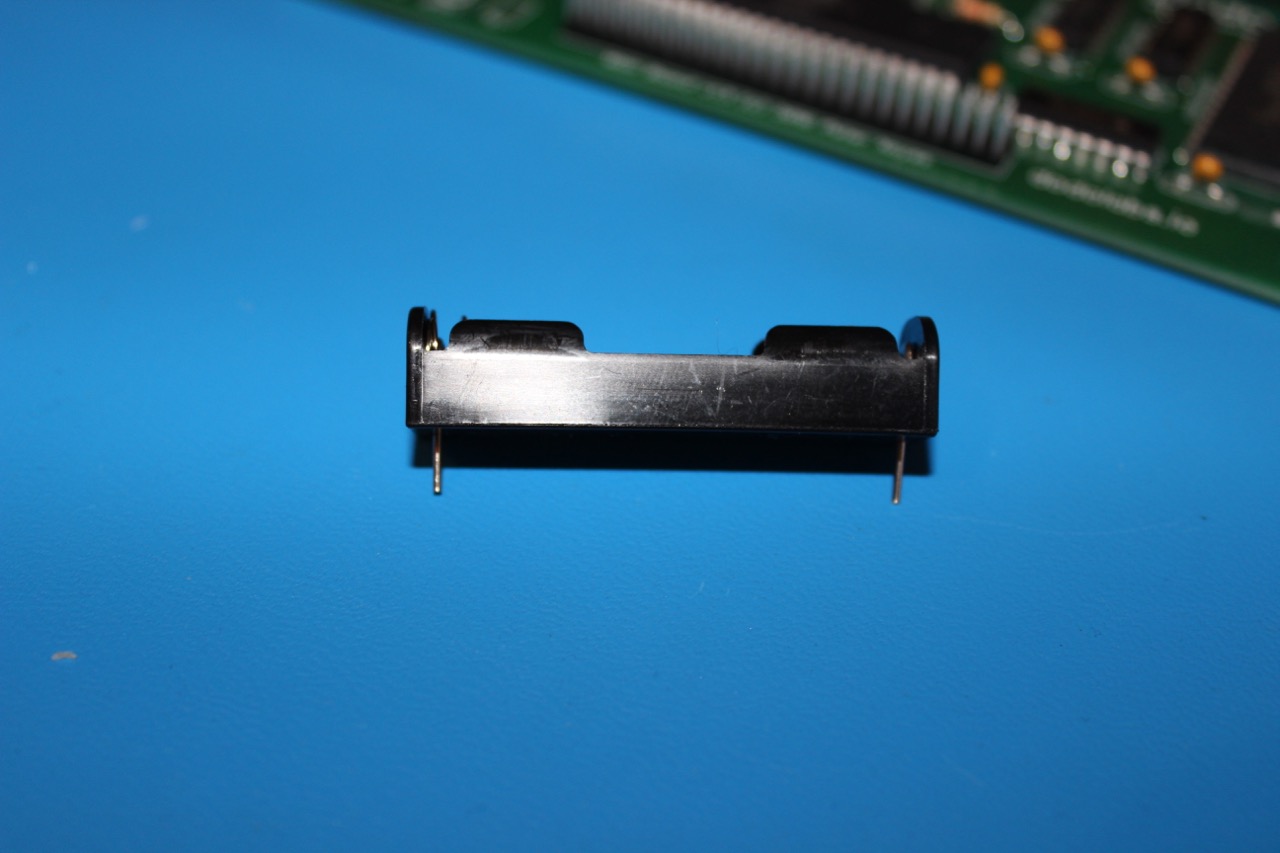
To position the battery holder in place while soldering, either use a helping hands tool as shown, or place something a few millimeters tall under the board so that they battery holder can rest in place.
Allow a large amount of solder to flow so that entire pad is covered and the leads are encased in solder, this is to ensure that there is a strong mechanical connection for the battery holders.
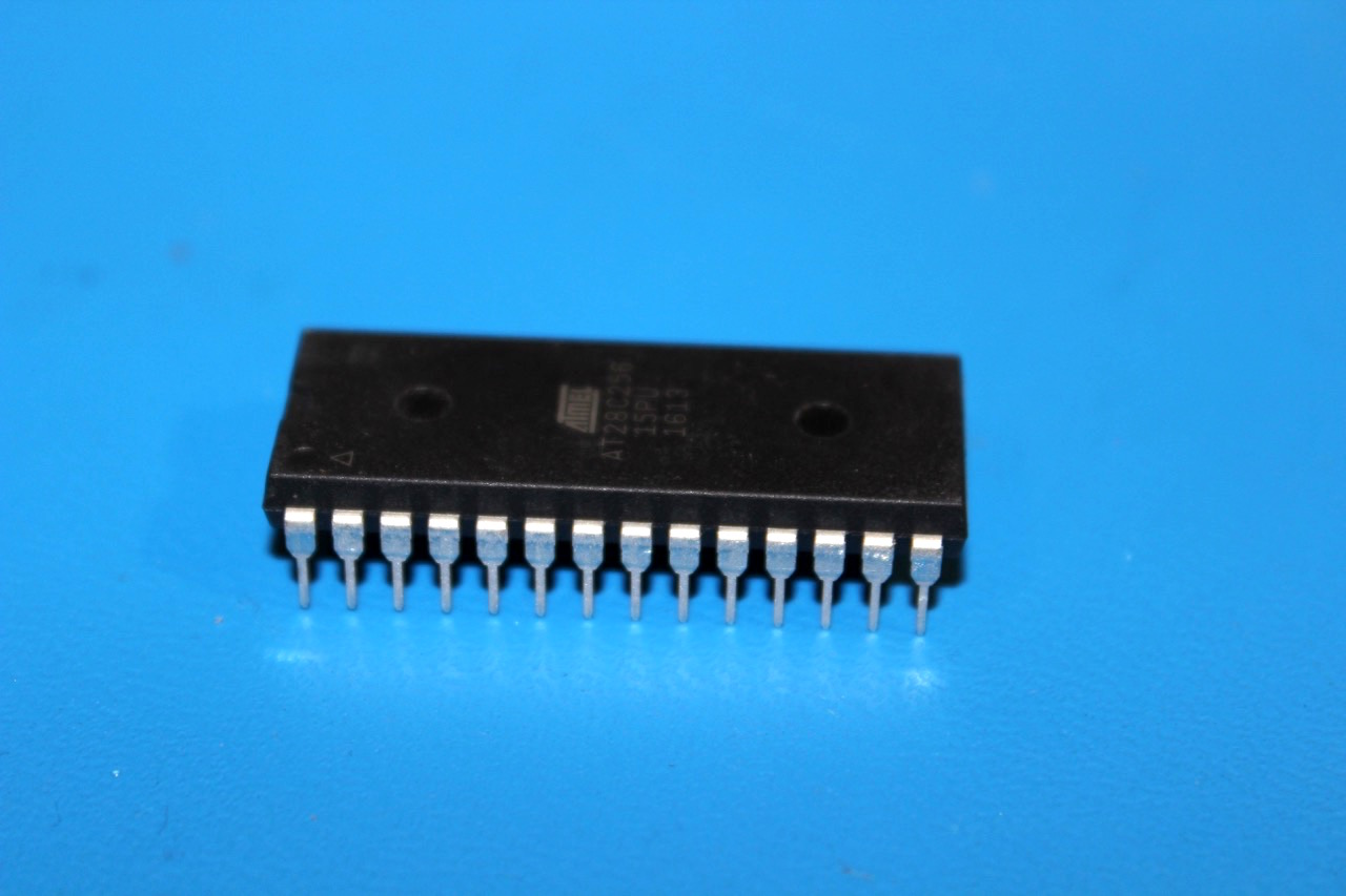
Step 13 - AT28C256 EEPROM
The final step for completing the mainboard is to install the EEPROM into the IC socket. Just as inserting the other ICs, the pins need to be bent slightly inward. Ensure the correct orientation of the chip and gently insert into the socket making sure no pins bend under the chip. To remove the chip use something like flat head screwdriver to evenly pry it up. Prying the chip out by hand will result in bent pins.
Complete
To jump straight to the I/O board assembly instuctions click here.