Glue Logic
Circuit Diagram
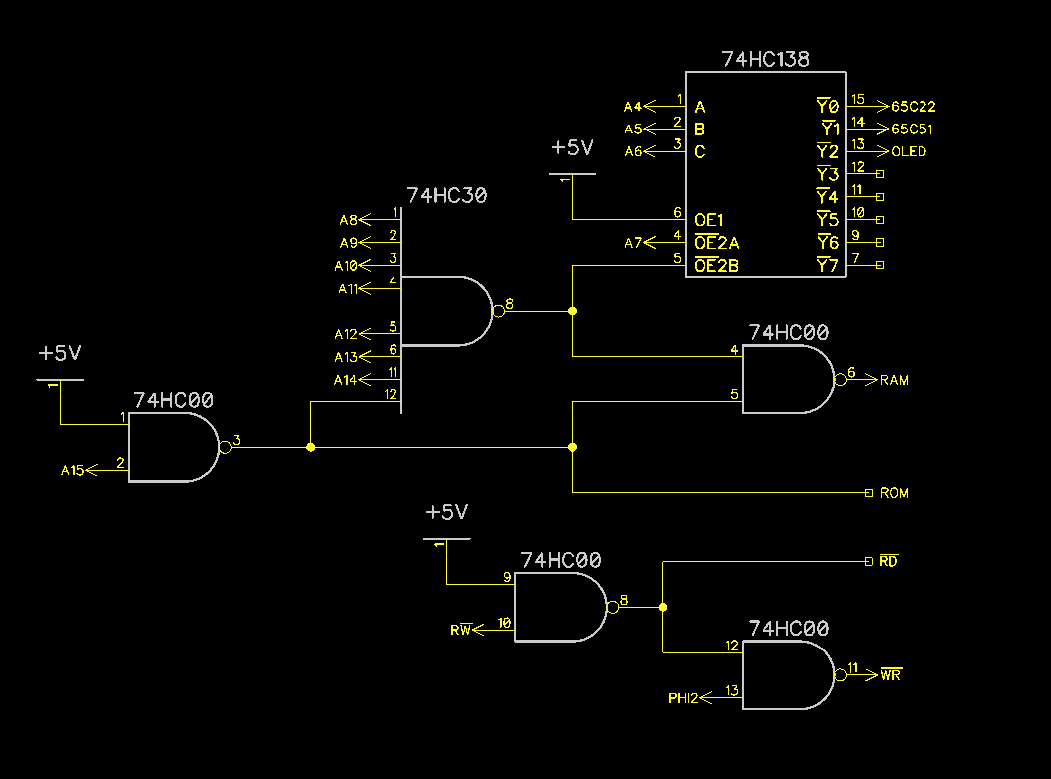
Background
A critical aspect of a 6502 based system is the layout of the address space. Glue logic is what determines the address space by enabling specific chips based upon particular addresses. For instance ROM lies in the upper 32KB of Dodo’s address space, therefore any time that A15 is high, ROM should be selected. By looking at the circuit diagram, A15 and 5V are fed into a NAND gate so that the ROM select goes low when A15 is high. Chip selection uses on active low logic. 3 distinct 74 series logic chips provide the necessary glue logic to lay out the following address space.
As a more complicated example examine the 8 input NAND gate. When A8-A14 are high, and the output of the ROM select is high (meaning that ROM is NOT selected), the output of the NAND represents one of the I/O chips being enabled. This means that when A15 is low, A8-A14 are high and the rest are low, that number equates to 0x7F00, the start of the I/O address space range.
Address Space
- 0x0000 - 0x7EFF : RAM
- 0x7F00 - 0x7F0F : 65C22
- 0x7F10 - 0x7F1F : 65C51
- 0x7F20 - 0x7F2F : SSD1305 (OLED Display)
- 0x7F30 - 0x7F7F : Reserved for future use
- 0x8000 - 0xFFFF : ROM
Components
| Component | Description | Image |
|---|---|---|
| 74HC138 | 3-8 Decoder | 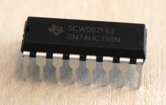 |
| 74HC00 | 4 2 input NAND gates | 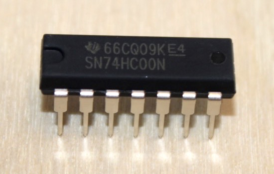 |
| 74HC30 | 8 input NAND gate | 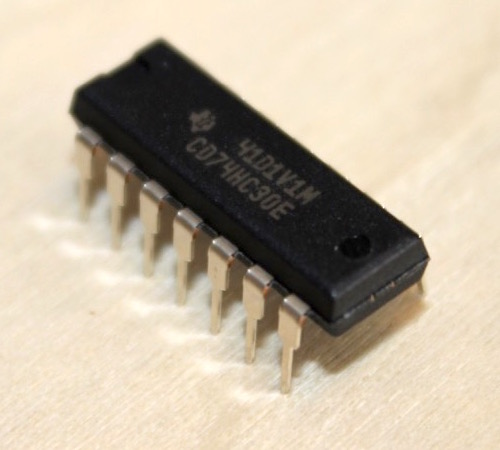 |